TSMC to Build $2.87 Billion Facility For Advanced Chip Packaging
by Anton Shilov on July 25, 2023 8:00 AM EST- Posted in
- Semiconductors
- TSMC
- Packaging
- CoWoS
- InFO
TSMC on Tuesday announced plans to construct a new advanced chip packaging facility in Tongluo Science Park. The company intends to spend around $2.87 billion on the fab that will employ some 1,500 people when it becomes operational several years from now.
"To meet market needs, TSMC is planning to establish an advanced packaging fab in the Tongluo Science Park," a statement by TSMC reads. "TSMC expects to invest nearly NT$90 billion for the project, and create 1,500 job opportunities. The Science Park Administration has officially agreed to TSMC's application to lease land at the Tongluo Science Park, and is arranging for a lease briefing."
The chip packing site itself is not expected to come online for several years. TSMC has yet to even begin ground preparations, and while the company isn't announcing a formal date for project completion, local Taiwanese media has been reporting that the fab will come online some time in 2027.
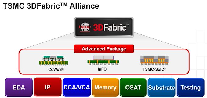
Otherwise, the nearly $2.9 billion price tag implies that this will be yet another significant capital expansion project for TSMC – rivaling what would have been the cost of a wafer lithography fab a decade ago. Given TSMC's product roadmaps as well as projections for the growing need for advanced packaging types in the coming years, the new chip packaging plant will likely be a comprehensive facility offering 3DFabric integration of front-end to back-end processes, as well as testing services.
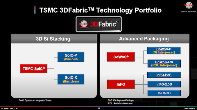
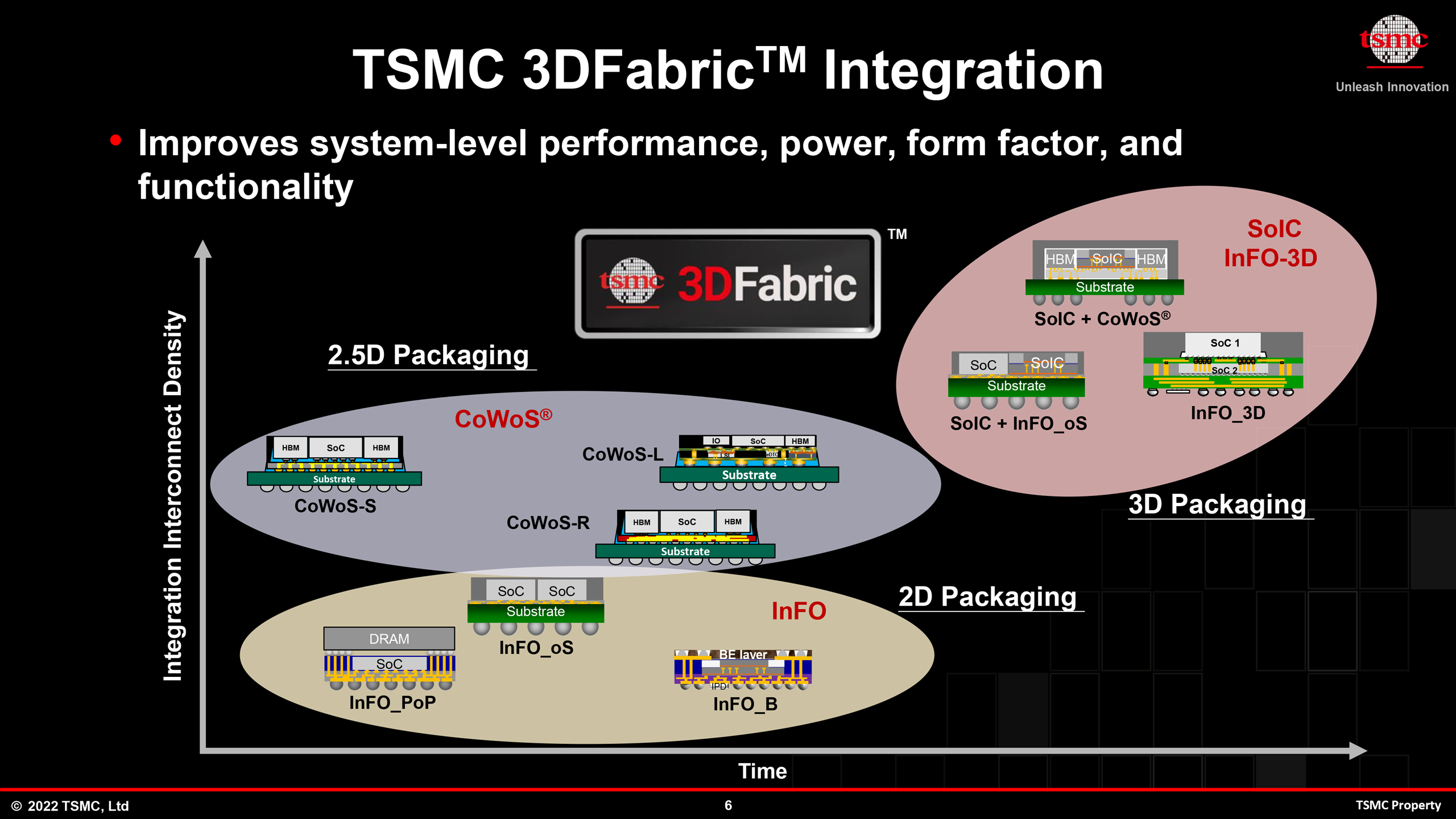
It is likely that the new Tongluo fab will be akin TSMC's recently opened Advanced Backend Fab 6 that is designed to support TSMC-SoIC (System on Integrated Chips) process technology, which includes such frontend 3D stacking techniques as chip-on-wafer (CoW) and wafer-on-wafer (WoW) as well as such backend packaging technologies like integrated fan-out (InFO) and chip-on-wafer-on-substrate (CoWoS).
TSMC's InFO and CoWoS packaging technologies are currently used for chips like Apple's M2 Ultra, AMD's Instinct MI300, and NVIDIA's A100 and H100 GPUs. Demand for the latter is booming these days and TSMC admitted just last week that the company barely has enough CoWoS capacity to meet it. As things stand, the company is working hard to double its CoWoS capacity by the end of 2024.
"But for the back end, the advanced packaging side, especially for the CoWoS, we do have some very tight capacity to — very hard to fulfill 100% of what customers needed," said C.C. Wei, chief executive of TSMC, at the company's earnings call last week. "So we are working with customers for the short term to help them to fulfill the demand, but we are increasing our capacity as quickly as possible. And we expect these tightness somewhat be released in next year, probably towards the end of next year. […] I will not give you the exact number [in terms of processed wafers capacity], but CoWoS [capacity will be doubled in 2024 vs. 2023].
TSMC's Advanced Backend Fab 6 can process about one million 300-mm wafers per year, as well as handle over 10 million hours of testing per year. Production capacity of the upcoming packaging fab is unknown, though it is reasonable to expect TSMC to make it even bigger as importance of advanced packaging is growing.


3 Comments
View All Comments
BushLin - Tuesday, July 25, 2023 - link
Tongluo Science Park is in Northern Taiwan. Everyone knows that, right? No way I had to look that up just now.RedGreenBlue - Saturday, July 29, 2023 - link
Started reading and then skimmed the whole article looking for it. Thanks for the legwork.RedGreenBlue - Saturday, July 29, 2023 - link
I kind of assumed though. Still wondering if they’ll build a packaging facility in the US.