Intel’s 11th Gen Core Tiger Lake SoC Detailed: SuperFin, Willow Cove and Xe-LP
by Dr. Ian Cutress on August 13, 2020 9:01 AM EST- Posted in
- CPUs
- Intel
- SoCs
- Tiger Lake
- 10+
- Xe-LP
- Willow Cove
- Intel Arch Day 2020
- SuperFin
- 10SF
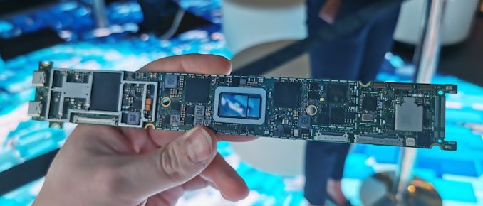
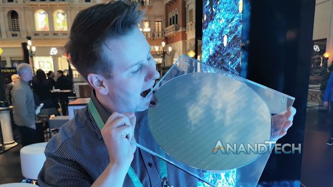
At the start of the year, Intel ‘foolishly’ handed me a wafer of its next generation Tiger Lake processors, as the moment it came into my hands I attempted to make a very quick exit. In my time with the wafer, we learned that this new 10nm laptop-focused processor had four cores, used Intel’s next generation Xe graphics architecture, and would set the stage at the end of the year as the cornerstone of Intel’s mobile processor offerings. As part of Intel’s Architecture Day 2020 a couple of days ago, the company went into detail about what makes Tiger Lake the true vehicle for 10nm, and why customers will want a Tiger Lake device.
Intel Architecture Day 2020, August 11th
Before we start into the information about Tiger Lake, I want to start by saying that the information in this article, as well as our coverage on Xe graphics and a number of upcoming mini-stories, all stems from Intel’s Architecture Day 2020 event. Building upon the success of the event in 2018, press and enthusiasts alike have continually asked when Intel would be doing it again. No doubt trying to pin down 20+ senior engineers and executives for an event at the same time in the same location is tough, and due to COVID this event was delayed at least twice.
Despite this, Intel made Arch Day 2020 a virtual event, allowing the engineers to pre-record their segments. The event was held behind closed doors, as with the 2018 event, the embargo lift was set for 1-2 days after. As a result, the articles you see published today are at the end of a lack of sleep between the event and now, as Intel went very dense very quickly (that’s a good thing™). We’ve digested as much as we can in that short space of time, we’ve asked some initial questions, but no doubt more will be asked as further analysis occurs.
The event was headlined by an effervescent Raja Koduri, who took the role of covering roadmaps and some of the Xe structural details. Prominent Intel Fellows and Engineers were the stars of the show in my eyes, particularly Ruth Brain (transistors), Ramune Nagisetty (packaging), Boyd Phelps (Tiger Lake), David Blythe (Xe GPU), Lisa Pierce (GPU software), Sailesh Kottapalli (Xeon) and others, all covering aspects of Intel’s strategy and portfolio.
Along with this article today covering Tiger Lake, we have an article going into the Xe graphics disclosures today as well. There are a number of mini-highlights from the event I also want to cover, and these will be published over the next few days.
Intel’s 11th Gen Core Tiger Lake SoC Detailed: Willow Cove and Xe-LP
Timeline: Tiger Lake will be Intel’s 11th Gen Core
Intel first unveiled its Core microarchitecture in Q1 2006, as an offshoot of the more power efficient Pentium Pro products. This was decided because the leading edge Intel products of the day, based on Netburst, were fast but hot and power hungry. By going down the route of Core, starting with Conroe, Intel has delivered multiple generations of products with the goal at each step to improve performance, power efficiency, and introduce better ways to perform compute.
| Intel's Core Family | |||||
| Gen | Year | Process | Core | Graphics | SoC |
| 1st Gen Core | 2006 | 65nm | Conroe | - | Core 2 |
| 2008 | 45nm | Nehalem | - | Lynnfield | |
| 2010 | 32nm | Westmere | Gen5 | Clarkdale | |
| 2nd Gen Core | 2011 | 32nm | Sandy Bridge | Gen6 | Sandy Bridge |
| 3rd Gen Core | 2012 | 22nm | Ivy Bridge | Gen7 | Ivy Bridge |
| 4th Gen Core | 2013 | 22nm | Haswell | Gen7.5 | Haswell |
| 5th Gen Core | 2015 | 14nm | Broadwell | Gen8 | Broadwell |
| 6th Gen Core | 2015 | 14nm | Skylake | Gen9 | Skylake |
| 7th Gen Core | 2017 | 14+ | Kaby Lake | Gen9 LP | Kaby Lake |
| 8th Gen Core | 2017 | 14++ | Coffee Lake | Gen9 LP | Coffee Lake |
| 2017 | 10 minus | Palm Cove | Gen10* | Cannon Lake | |
| 2018 | 14++ | Whiskey Lake | Gen9 LP | Whiskey Lake | |
| 2019 | 14+ | Amber Lake | Gen9 LP | Amber Lake | |
| 9th Gen Core | 2018 | 14++ | Coffee Lake | Gen9 LP | Coffee Lake-R |
| 10th Gen Core | 2019 | 14+++ | Comet Lake | Gen9 | Comet Lake |
| 2019 | 10nm | Sunny Cove | Gen11 | Ice Lake | |
| 11th Gen Core | 2020 | 10SF | Willow Cove | Xe-LP | Tiger Lake |
| *Cannon Lake's Gen10 was never enabled | |||||
[table – year, generation, process node, core, soc]
Intel uses a lot of code names for its cores and for its products. The marketable names that get printed on the side of the retail box are do with ‘9th Generation Core’, however because we are dealing with the finer details of these products and cores, we prefer to use the code names. Keep this cheat sheet if the number of code names starts getting dense.
Tiger Lake pairs Willow Cove with Xe-LP
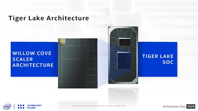
At its heart, the current Tiger Lake processor being presented by Intel is a four core mobile-series processor aimed at the 15 W target market where premium ultra-portable notebooks exist. Inside is four cores based on Intel’s Willow Cove architecture, the next generation after Sunny Cove, which we saw in Ice Lake. The four cores will be paired with 96 Execution Units of the new Xe-LP graphics architecture, and Tiger Lake will be Intel’s first product with Xe-LP.
Compared to Intel’s current generation product in this space, its Ice Lake processor, the number of CPU cores stays the same, but we move from a Sunny Cove core design to a Willow Cove core design, which has performance benefits we will detail later. Graphics is boosted in raw numbers by +50%, moving from 64 EUs to 96 EUs, however the architecture change from Ice Lake’s Gen11 design to the new Xe-LP affords additional performance benefits.
Tiger Lake also includes on-silicon support for technologies such as Thunderbolt 4, USB 4, PCIe 4.0, LPDDR5, as well as dedicated IP for total memory encryption and an updated Gaussian Neural Accelerator (to help with noise cancellation and similar functionality). We cover these on our page about Tiger Lake’s IO and sub-system.
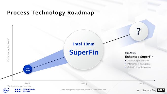
No Longer on 10+, new 10nm SuperFin Technology
Tiger Lake uses Intel’s 10nm ‘SuperFin’ manufacturing process technology. As part of this launch, Intel has replaced the 10+ nomenclature and instead renamed it to 10nm SuperFin, or 10SF. This is in part due to some of the updates Intel has made to its 10nm process in order to enable some of the features in Tiger Lake.
The SuperFin technology includes a new high performance transistor methodology for the critical paths of Intel’s design, and an improved metal stack which uses novel materials in the latest update to Intel’s FinFET process technology. This includes evolutionary changes to achieve the required performance characteristics that perhaps should have been part of Intel’s 10nm process from the beginning.
We will also cover the new SuperFin over the course of our Intel Architecture Day coverage.
Intel has also renamed the generation after 10nm SuperFin, and called it 10nm Enhanced SuperFin, or 10ESF for short. This comes into play with some of Intel’s future products, such as its high performance computing GPU called Ponte Vecchio, as well as the next generation Xeon Scalable platform called Sapphire Rapids.
Tiger Lake Goals: Bigger and Better than Ice Lake
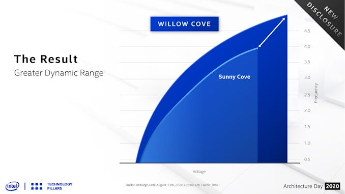
As part of Intel’s disclosures about Tiger Lake and specifically to talk on Willow Cove, Intel’s Boyd Phelps, the Tiger Lake SoC Lead Architect, spoke about how the new design, coupled with the new manufacturing technology, enables the new core to offer better performance and better performance efficiency at every point of the curve compared to Ice Lake.
As part of the design of Tiger Lake, Intel had two options on how to build on the Ice Lake design: push further with better single thread performance / IPC, or drive performance and efficiency. Intel ultimately focused more on the latter, as the engineers felt that it would enable a bigger leap in performance over the Ice Lake design.
This means that the new cores in Tiger Lake a built that for any given power or voltage, they will run at a higher frequency. Or for any given frequency, Tiger Lake will require a lower voltage. Where Ice Lake essentially topped out at 4.0 GHz within that 15 W window, Tiger Lake will start pushing numbers back up to 5.0 GHz.
This is important – when we reviewed Ice Lake, it was a bit of an odd situation. At the time, Intel’s main comparison point was its previous generation Whiskey Lake processors. Ice Lake afforded a raw 15-20% performance uplift against Whiskey Lake at the same frequency, which in general is a very good metric to have. However, Ice Lake was 10-20% lower on frequency, effectively nullifying all of those gains. At the same power, Ice Lake had a hard time beating the previous generation.
With Tiger Lake then, the stage seems to be set that the raw performance in frequency alone is going to jump anywhere from 10-20% depending on how the turbo modes are set to work in the final products. Intel puts this improvement in frequency down to its new SuperFin transistor design and updated manufacturing process.
When it comes to clock-for-clock raw performance gains for Tiger Lake, the differences compared to Ice Lake are not as clear cut, primarily because the cores microarchitecture layout between the two only has a few small changes. We’ll cover those a bit later.






71 Comments
View All Comments
Quantumz0d - Thursday, August 13, 2020 - link
"The others not mentioned will be split between 7nm and external fabs. More on that info in a separate article"So that means they are going for external fab really. Damn. What a shame. I wonder if that's the CPU or this GPU. Anything is a shame on Intel and that beancounter Bob.
IanCutress - Thursday, August 13, 2020 - link
That's referring to the other tiles of Ponte Vecchio. There are 4. We covered 2.Eliadbu - Thursday, August 13, 2020 - link
Shame is when you don't acknowledge your problems and how they might limit you. Going with external fabs allows the company to be competitive where it needs the most. But they sure need a long term strategy and and make critical decisions like which processes they would utilize earlier.Kangal - Thursday, August 13, 2020 - link
It's only GPU.And it's only the Xe-HP (ergo Discreet GPU) variant.
It seems to imply that is only on the 10SFE "enhanced" variant. Basically using TSMC 7nm process for the higher memory and connector chips, named as "Rambo Cache" and "Xe Link". And that's targeting the server market and high-end desktops (ie think Nvidia Titan).
Seems like Intel realise how embarrassing it is to ask for their competitors wafers for their main product, so instead they're taking a half-measure and using it for the GPU only. That way they get to save face and say "well, AMD and Nvidia do it too". Also it seems they couldn't get any good prices, which is why only some chips are made on the 7nm, and rest are made in-house on 10nm. Overall, this is Intel playing hard to catch up to TSMC's 7nm and AMD's Zen2 and AMD's Vega. That's why the whole thing is difficult to understand, as it is purposely obfuscated. Yet these will only ship in (late) 2021, whereas the competition is posied to actually leap ahead in 2020 to +7nm TSMC, Zen3, RDNA2. And when Intel arrives, they might even be facing off against 5nm and a Zen3+ refresh. Just to put things into perspective.
tipoo - Thursday, August 13, 2020 - link
This reads quite promising. Great writeup."A few angstroms thick" it's hard to even think about the scale of this stuff, that's 0.1 nanometres or 100 picometres. How far from atomic bonding limits?
DrJackMiller - Thursday, August 13, 2020 - link
It's pretty damn close, but that depends on the bond :-). For a perhaps more human comparison, that of O-O in Oxygen is 1.208 Å; and in C=O bonds (e.g. in CO2) it's around 1.16 Å.vortmax2 - Friday, August 14, 2020 - link
Would love to see an article here of the next 10-20 years of processors as we enter deeper into the atomic scale. What the next big breakthrough?jospoortvliet - Saturday, August 15, 2020 - link
Less promising is that they went for a four cores design again. With AMD pushing the desktop to 8 with the first Zen you would think they would realize amd would pull the same when going mobile and prepare for it... so is this arrogance thinking their cores are so much better or they control the market? Lack of strategic insight? Or inability to work out things for the yield and cost math?Spunjji - Monday, August 17, 2020 - link
If these cores are as good as they're claiming they are, there will be a legitimate dilemma choosing between 4 Very Fast cores and 8 Really Quite Fast cores.I'd wager that yields are 80% to blame and power is the rest - they have an 8-core Tiger in the works, but it's a 35/45W part and there's nothing firm about a release date yet.
none12345 - Tuesday, August 18, 2020 - link
Depends on the atoms, but for reference how about silicon."Silicon has the diamond cubic crystal structure with a lattice parameter of 0.543 nm. The nearest neighbor distance is 0.235 nm."
Diatomic hydrogen is the smallest molecule with a bond length of 0.74 angstrom.
Bond length is typically 1-2 angstrom.
"Intel states that this is an industry first/leading design, enabled through careful deposition of new Hi-K materials in thin layers, smaller than 0.1nm, to form a superlattice between two or more material types."
Unless im missing something, the above statement does not make any sense to me. thin layers of atoms less then the average bond length between atoms is nonsensical.