Hot Chips 31 Live Blogs: Cerebras' 1.2 Trillion Transistor Deep Learning Processor
by Dr. Ian Cutress on August 19, 2019 9:45 PM EST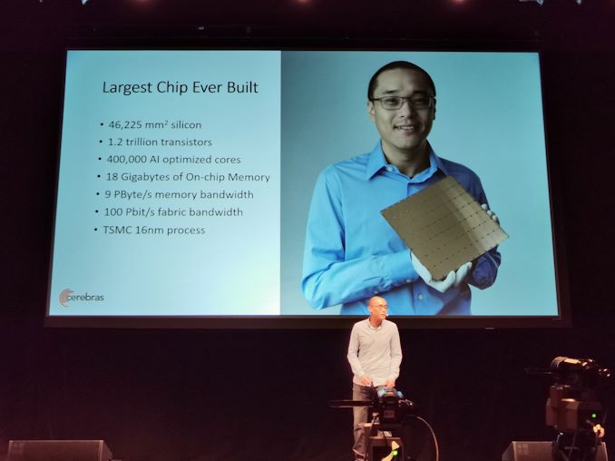
08:49PM EDT - Some of the big news of today is Cerebras announcing its wafer-scale 1.2 trillion transistor solution for deep learning. The talk today goes into detail about the technology.

08:51PM EDT - Wafer scale chip, over 46,225 mm2, 1.2 trillion transistors, 400k AI cores, fed by 18GB of on-chip SRAM
08:51PM EDT - TSMC 16nm
08:51PM EDT - 215mm x 215mm - 8.5 inches per side
08:51PM EDT - 56 times larger than the largest GPU today
08:52PM EDT - Built for Deep Learning
08:52PM EDT - DL training is hard (ed: this is an understatement)

08:52PM EDT - Peta-to-exa scale compute range
08:53PM EDT - The shape of the problem is difficult to scale
08:53PM EDT - Fine grain has a lot of parallelism
08:53PM EDT - Coarse grain is inherently serial
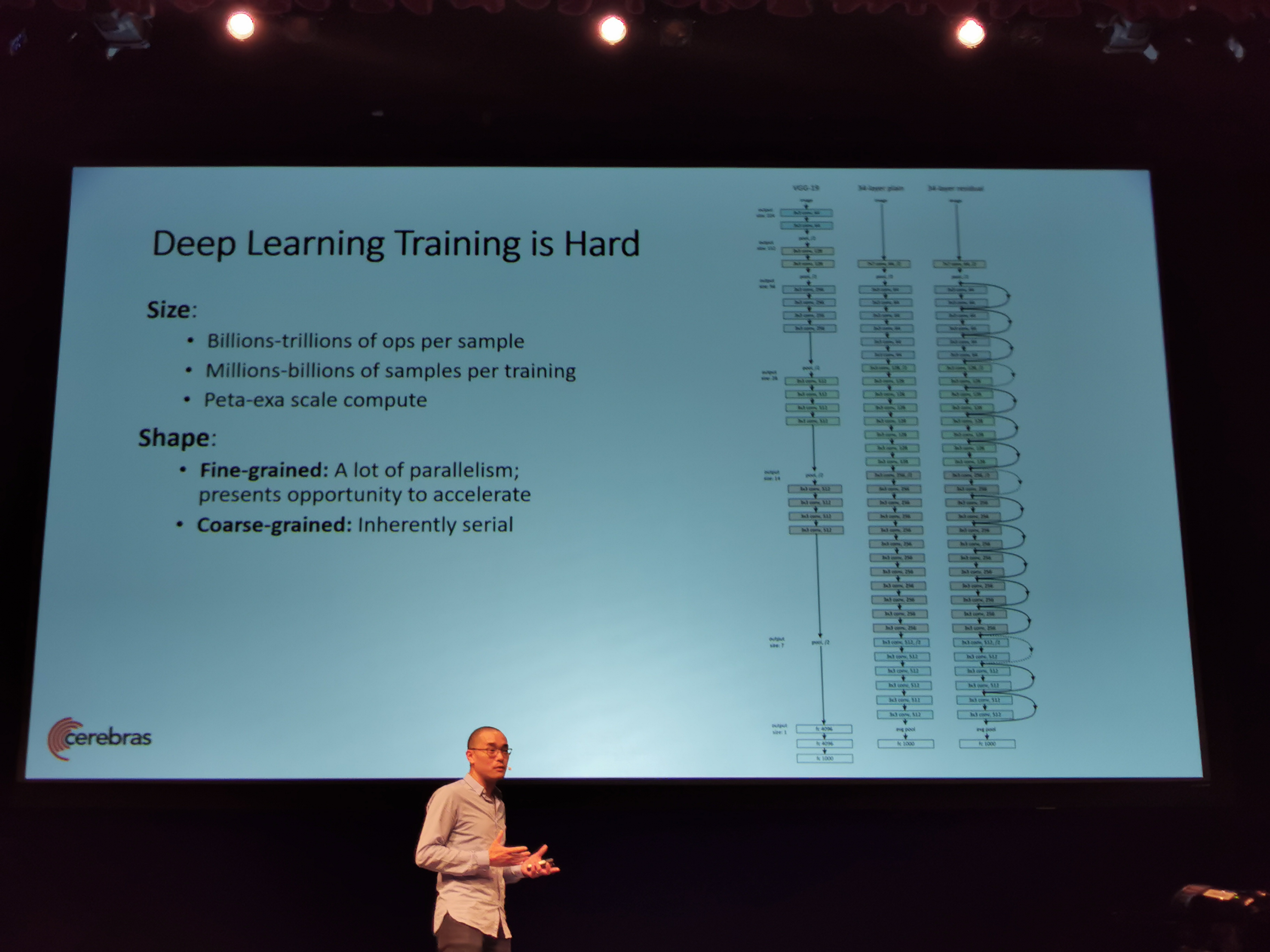
08:53PM EDT - Training is the process of applying small changes, serially
08:53PM EDT - Size and shape of the problem makes training NN really hard
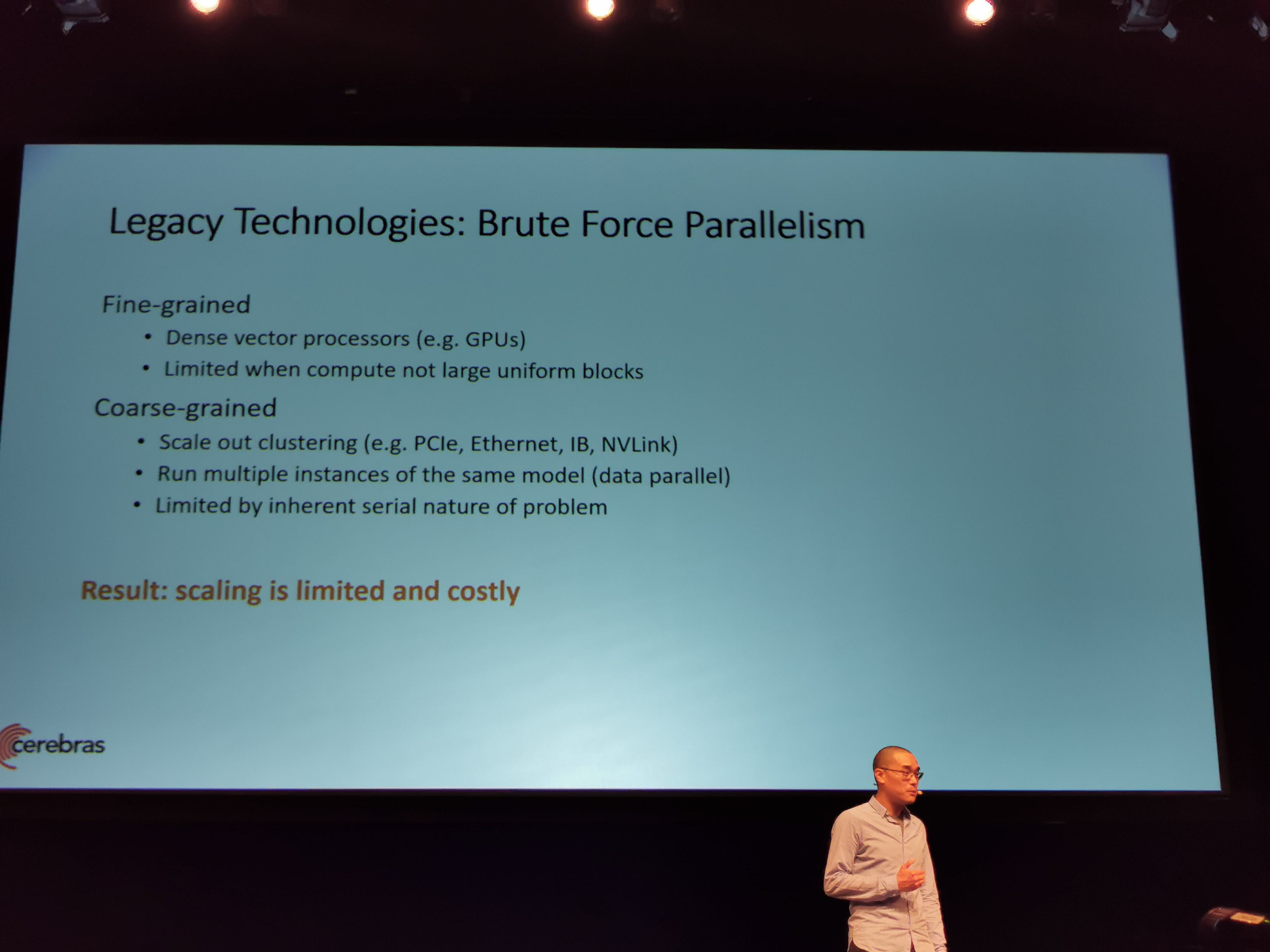
08:53PM EDT - Today we have dense vector compute
08:54PM EDT - For Coarse Grained, require high speed interconnect to run mutliple instances. Still limited
08:54PM EDT - Scaling is limited and costly
08:54PM EDT - Specialized accelerators are the answer
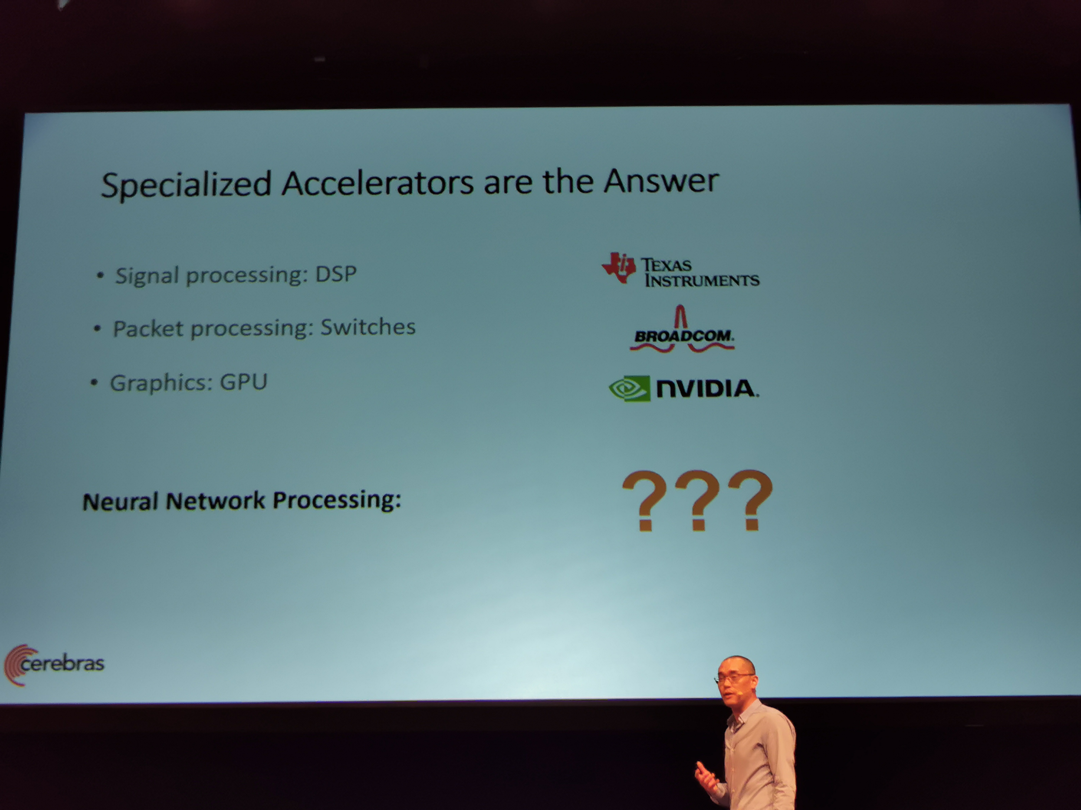
08:55PM EDT - NN: what is the right architecture
08:55PM EDT - Need a core to be optimized for NN primitives
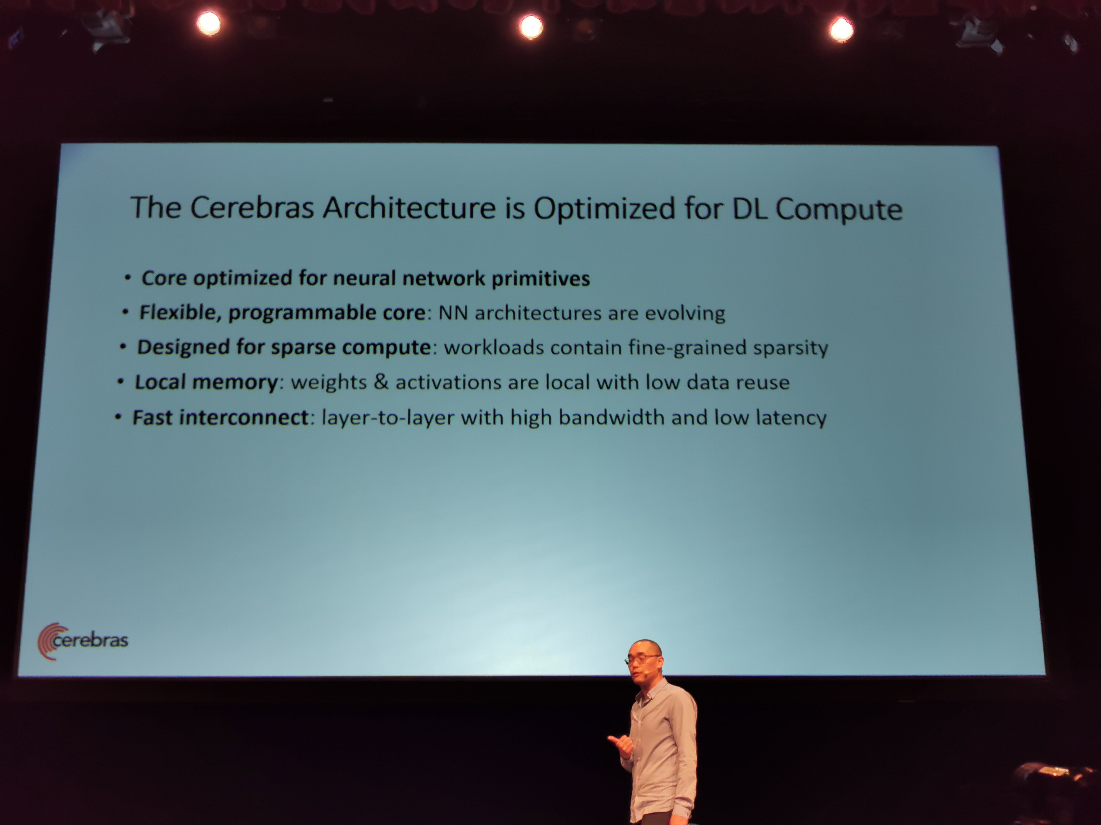
08:55PM EDT - Need a programmable NN core
08:55PM EDT - Needs to do sparse compute fast
08:55PM EDT - Needs fast local memory
08:55PM EDT - All of the cores should be connected with a fast interconnect
08:56PM EDT - Cerebras uses flexible cores. Flexible general ops for control processing
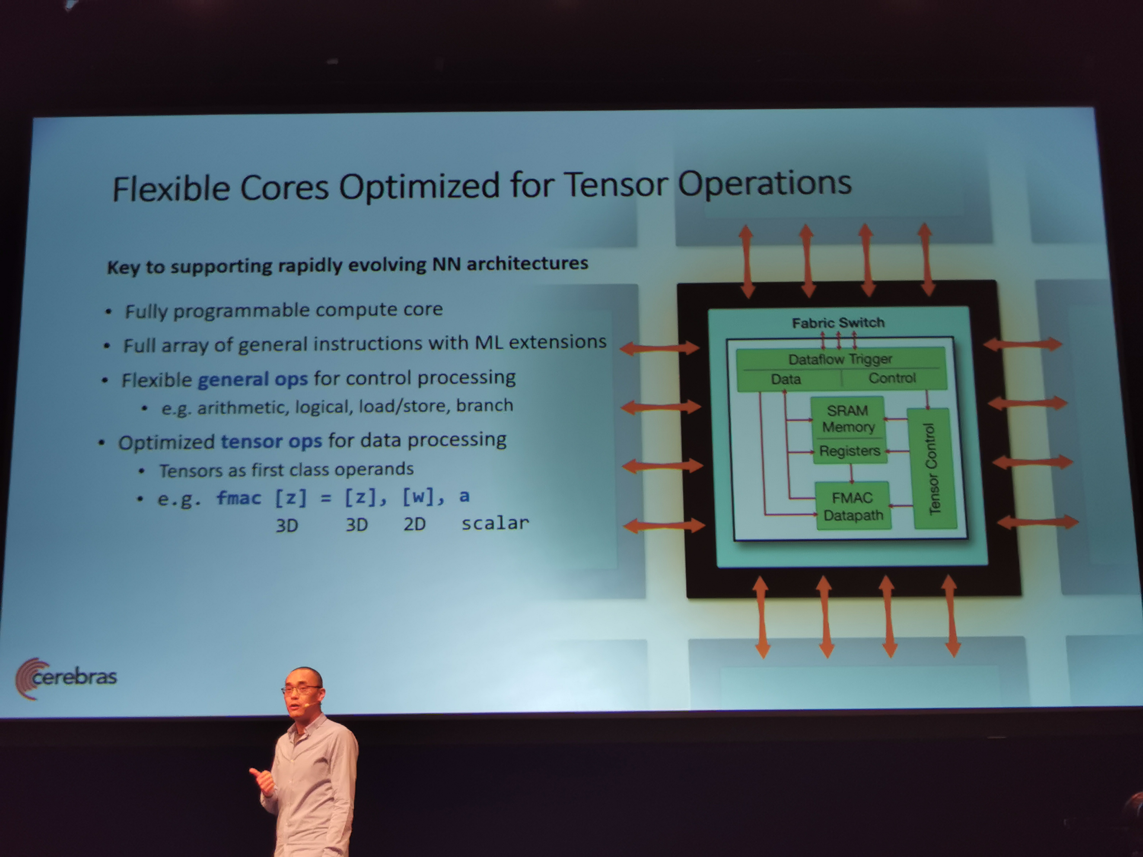
08:56PM EDT - Core should handle tensor operations very efficiency
08:56PM EDT - Forms the bulk fo the compute in any neural network
08:56PM EDT - Tensors as first class operands
08:57PM EDT - fmac native op
08:57PM EDT - NN naturally creates sparse networks
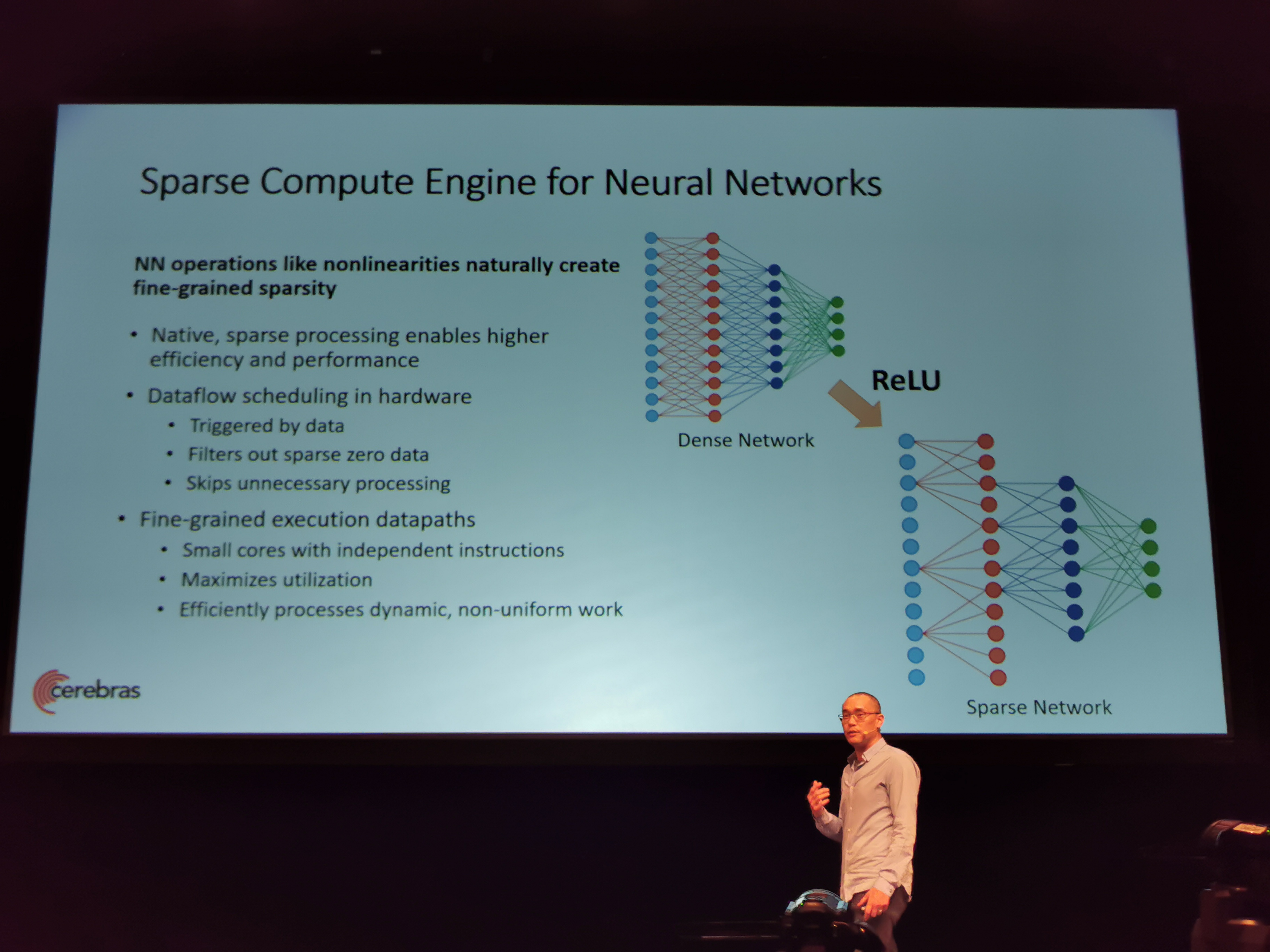
08:58PM EDT - The core has native sparse processing in the hardware with dataflow scheduling
08:58PM EDT - All the compute is triggered by the data
08:58PM EDT - Filters all the sparse zeros, and filters the work
08:58PM EDT - saves the power and energy, and get performance and acceleration by moving onto the next useful work
08:58PM EDT - Enabled because arch has fine-grained execution datapaths
08:58PM EDT - Many small cores with independent instructions
08:59PM EDT - Allows for very non-uniform work
08:59PM EDT - Next is memory
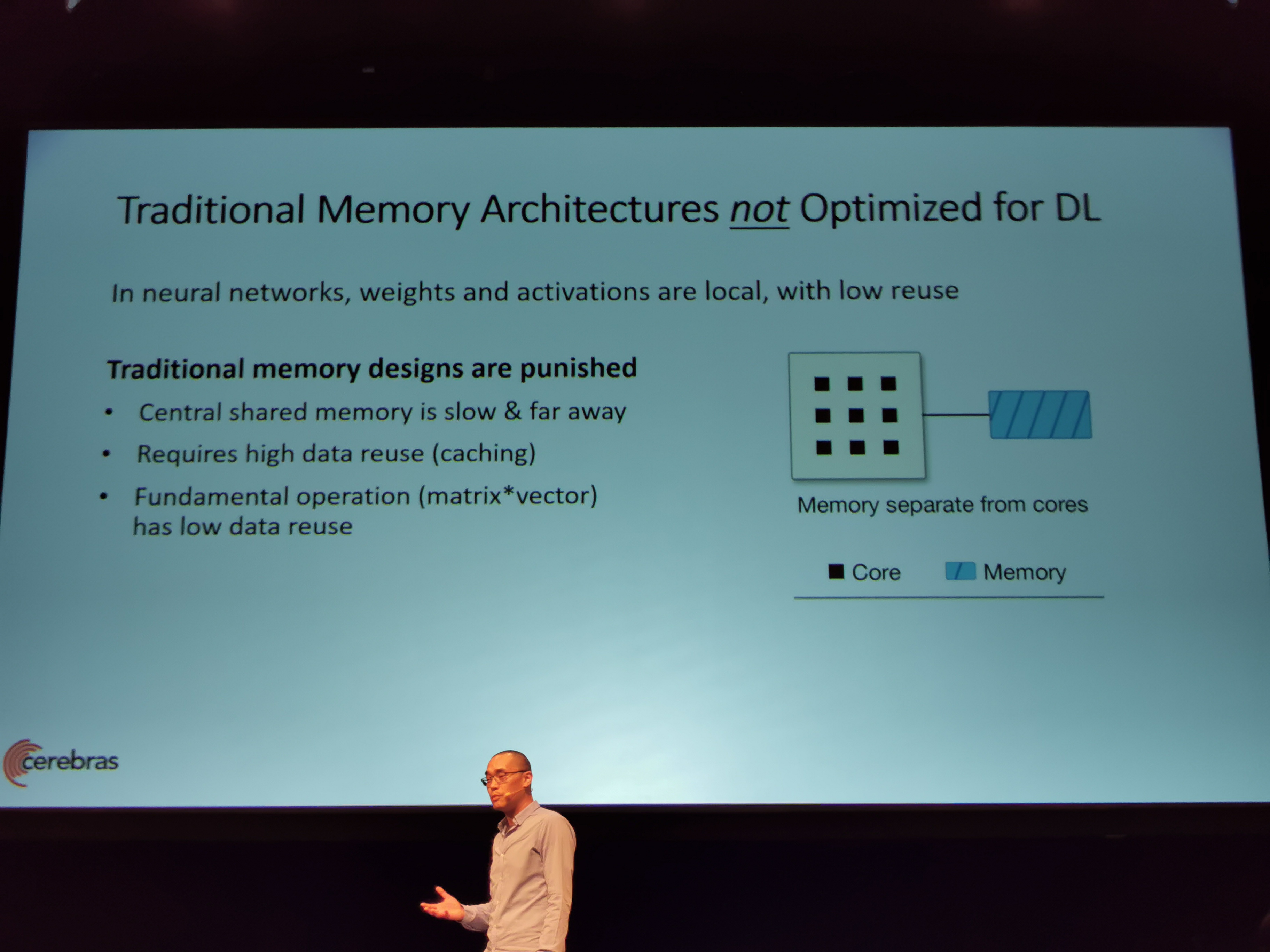
08:59PM EDT - Traditional memory architectures are not optimized for DL
08:59PM EDT - Traditional memory requires high data reuse for performane
09:00PM EDT - Normal matrix multiply has low end data reuse
09:00PM EDT - Translating Mat*Vec into Mat*Mat, but changes the training dynamics
09:00PM EDT - Cerebras has high-perf, fully distributed on-chip SRAM next to the cores
09:01PM EDT - Getting orders of magnitude higher bandwidth
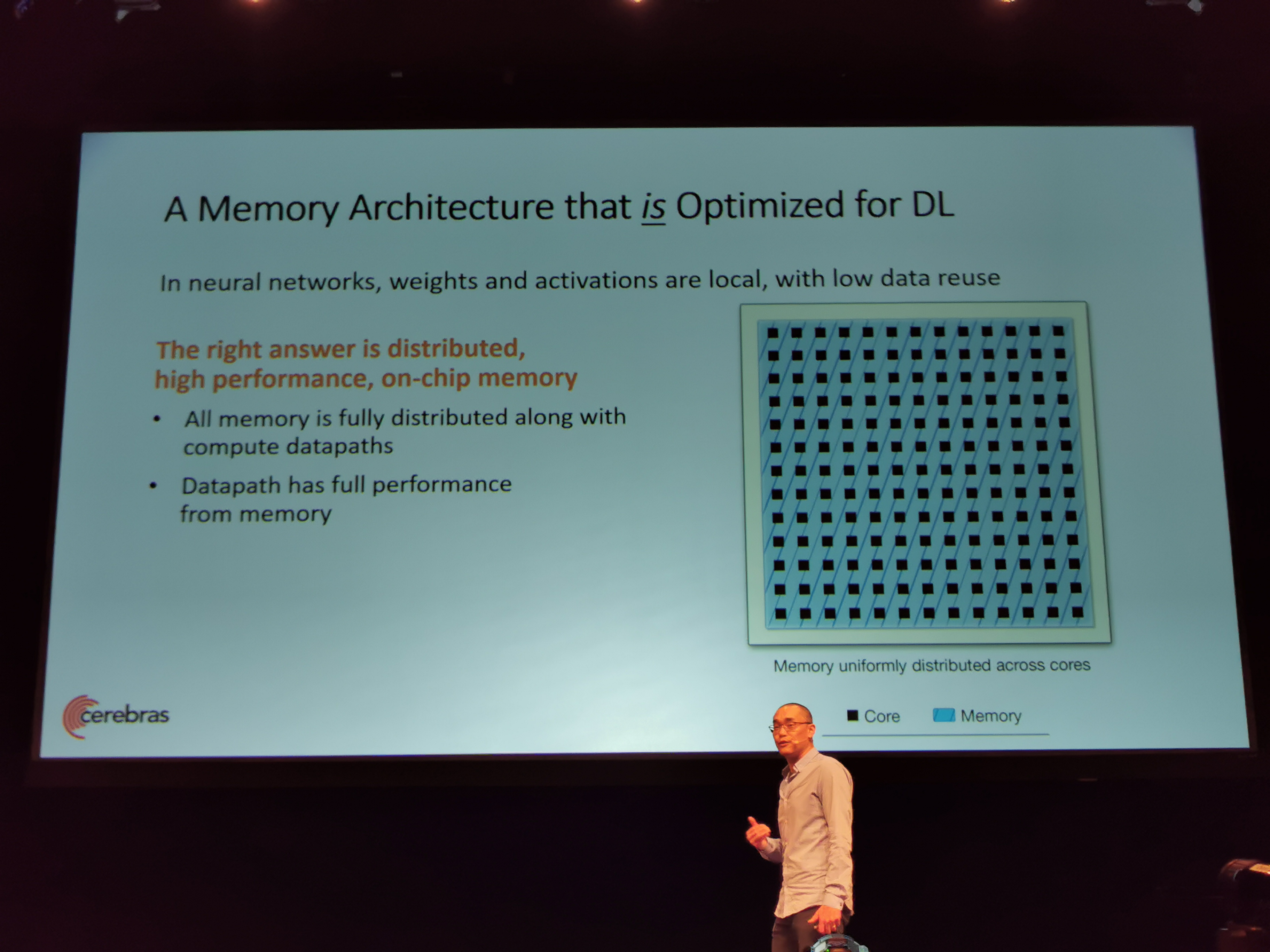
09:01PM EDT - ML can be done the way it wants to be done
09:01PM EDT - High bandwidth, low latency interconnect
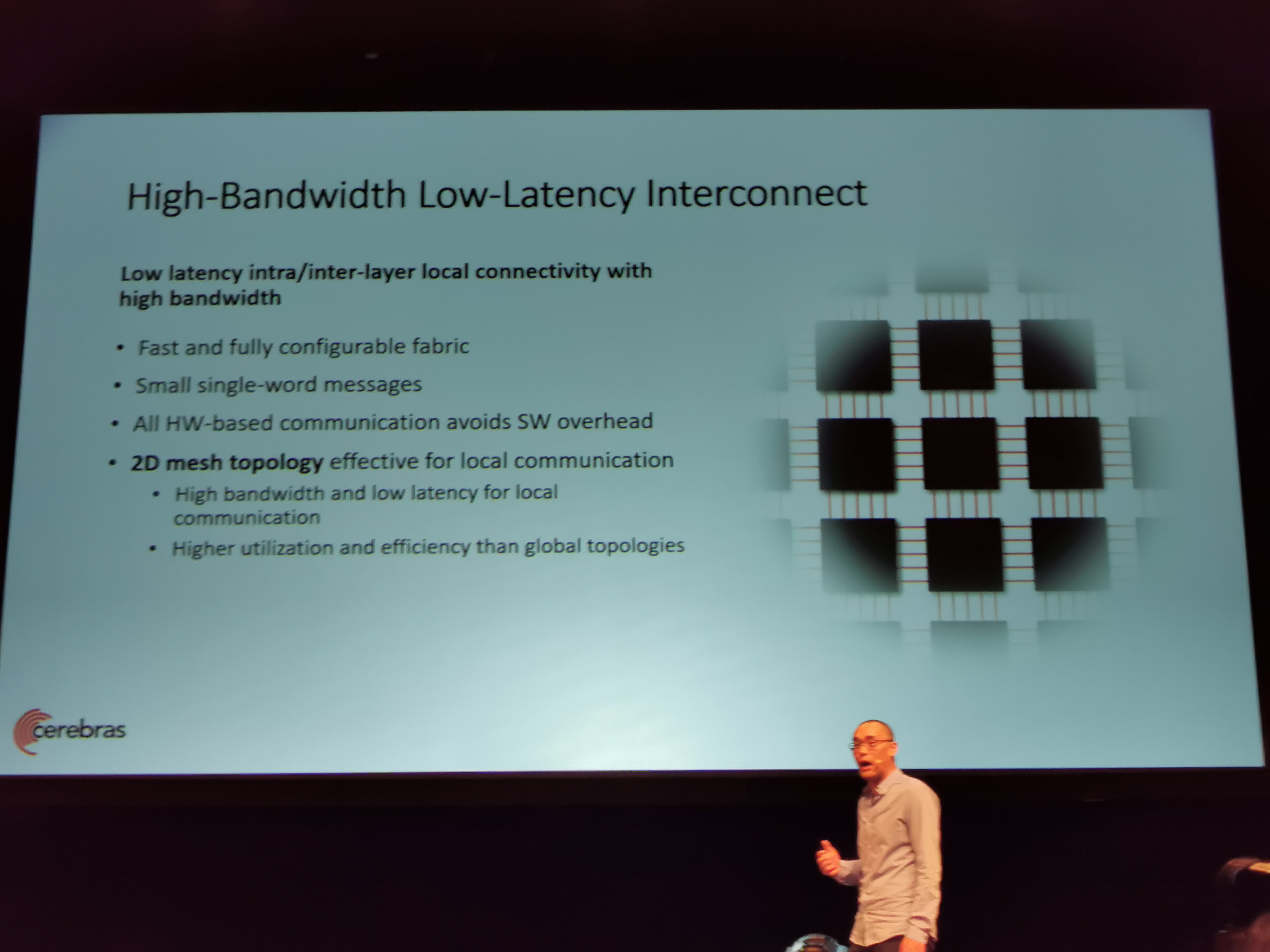
09:01PM EDT - fast and fully configurable fabric
09:01PM EDT - all hw based communication avoicd sw overhead
09:02PM EDT - 2D mesh topology
09:02PM EDT - higher utlization and efficiency than global topologies
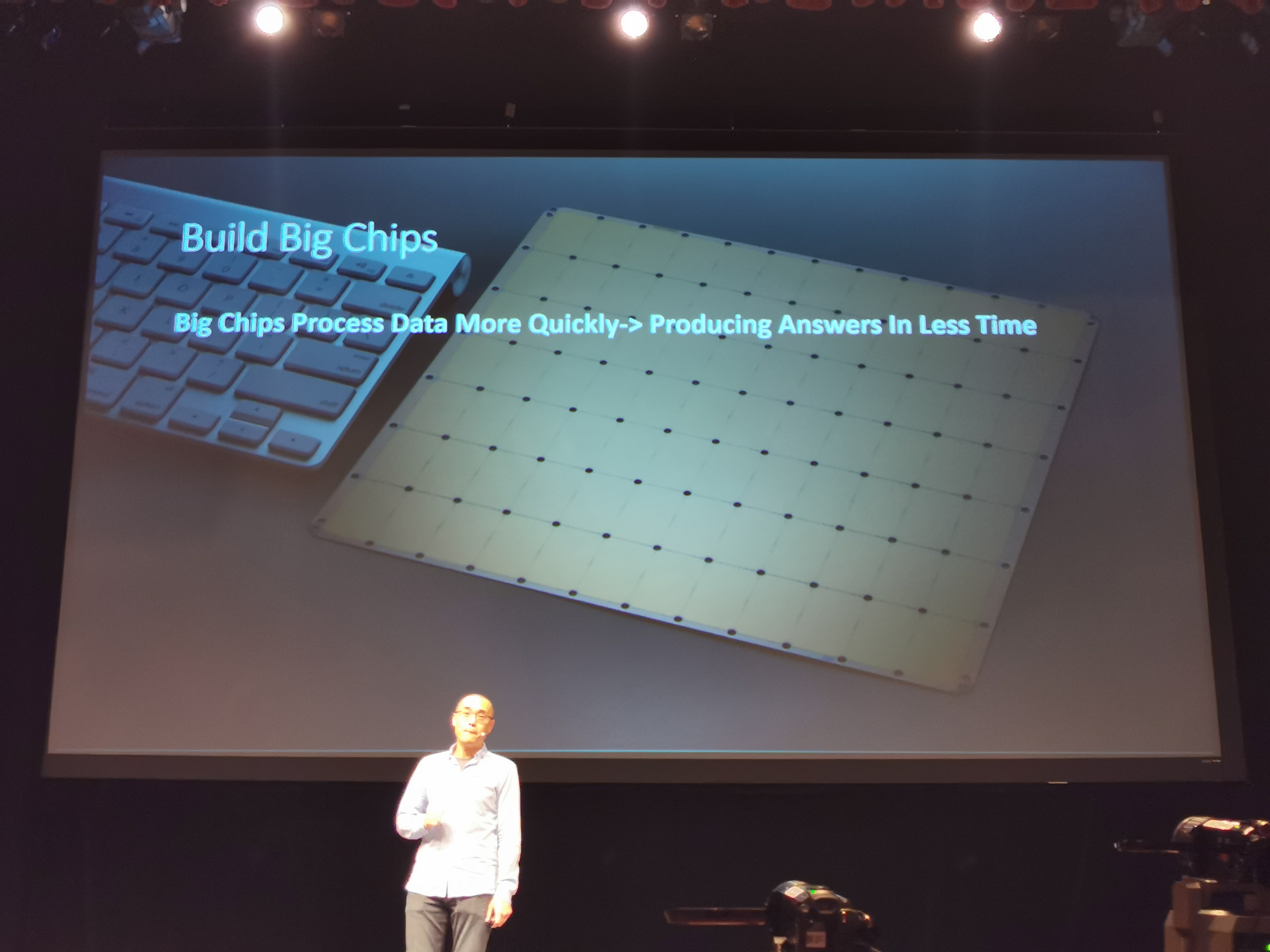
09:02PM EDT - Need more than a single die
09:02PM EDT - Solition is a wafer scale
09:03PM EDT - Build Big chips
09:03PM EDT - Cluster scale perf on a single chip
09:03PM EDT - GB of fast memory (SRAM) 1 clock cycle from the core
09:03PM EDT - That's impossible with off-chip memory
09:03PM EDT - Full on-chip interconnect fabric
09:03PM EDT - Model parallel, linear performance scaling
09:04PM EDT - Map the entire neural network onto the chip at once
09:04PM EDT - One instance of NN, don't have to increase batch size to get cluster scale perf
09:04PM EDT - Vastly lower power and less space
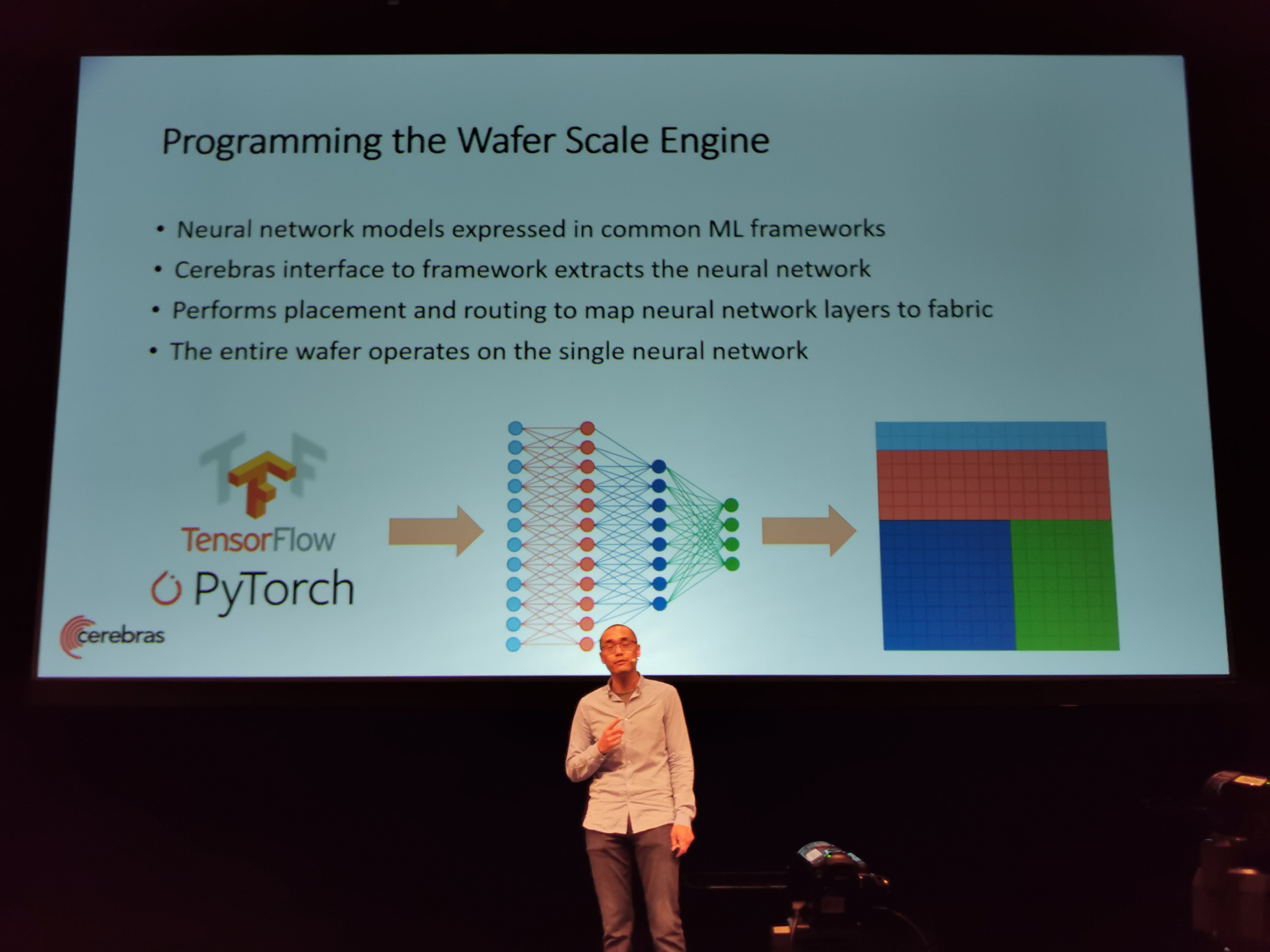
09:04PM EDT - Can use TensorFlow and PyTorch
09:05PM EDT - Performs placing and routing to map neural network layers to fabric
09:05PM EDT - Entire wafer operates on the single neural network
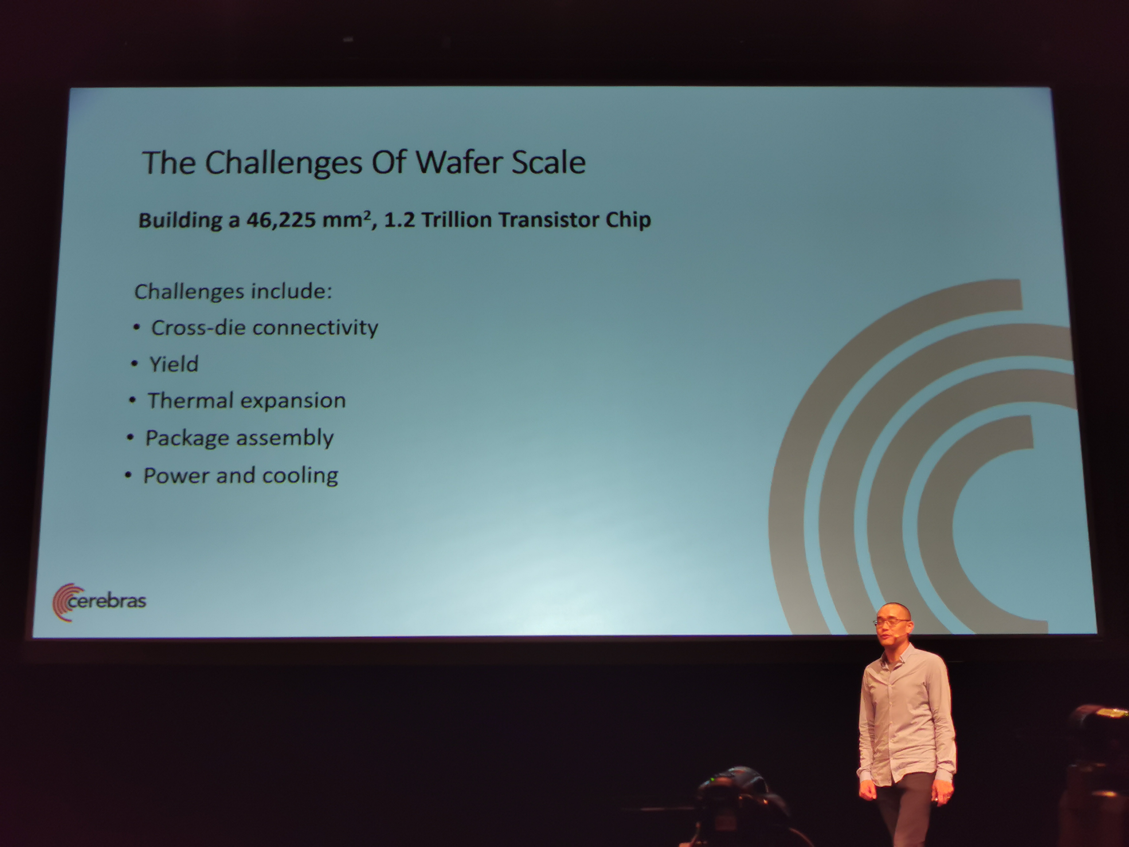
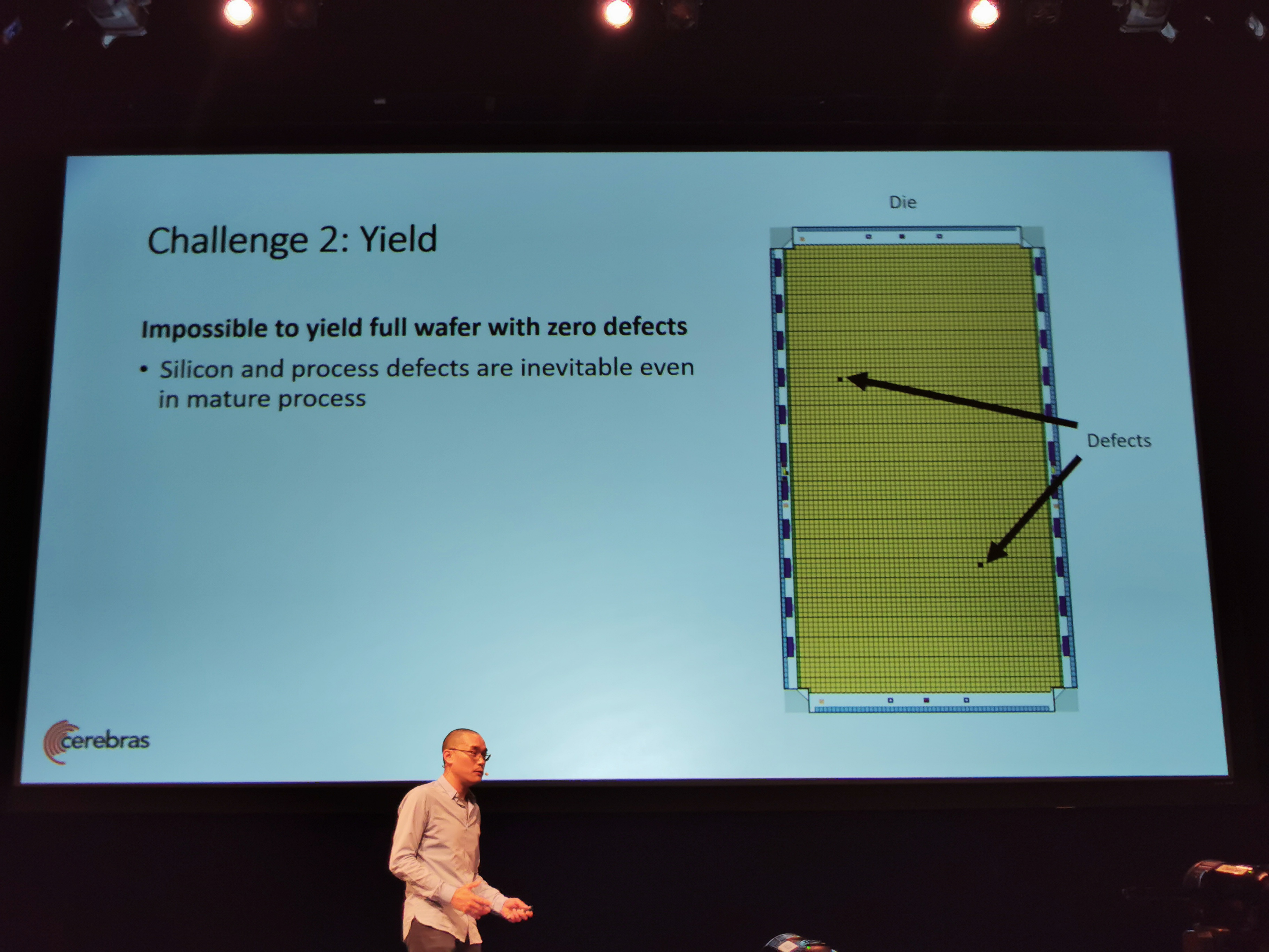
09:05PM EDT - Challenges of wafer scale
09:05PM EDT - Need cross-die connectivity, yield, thermal expansion
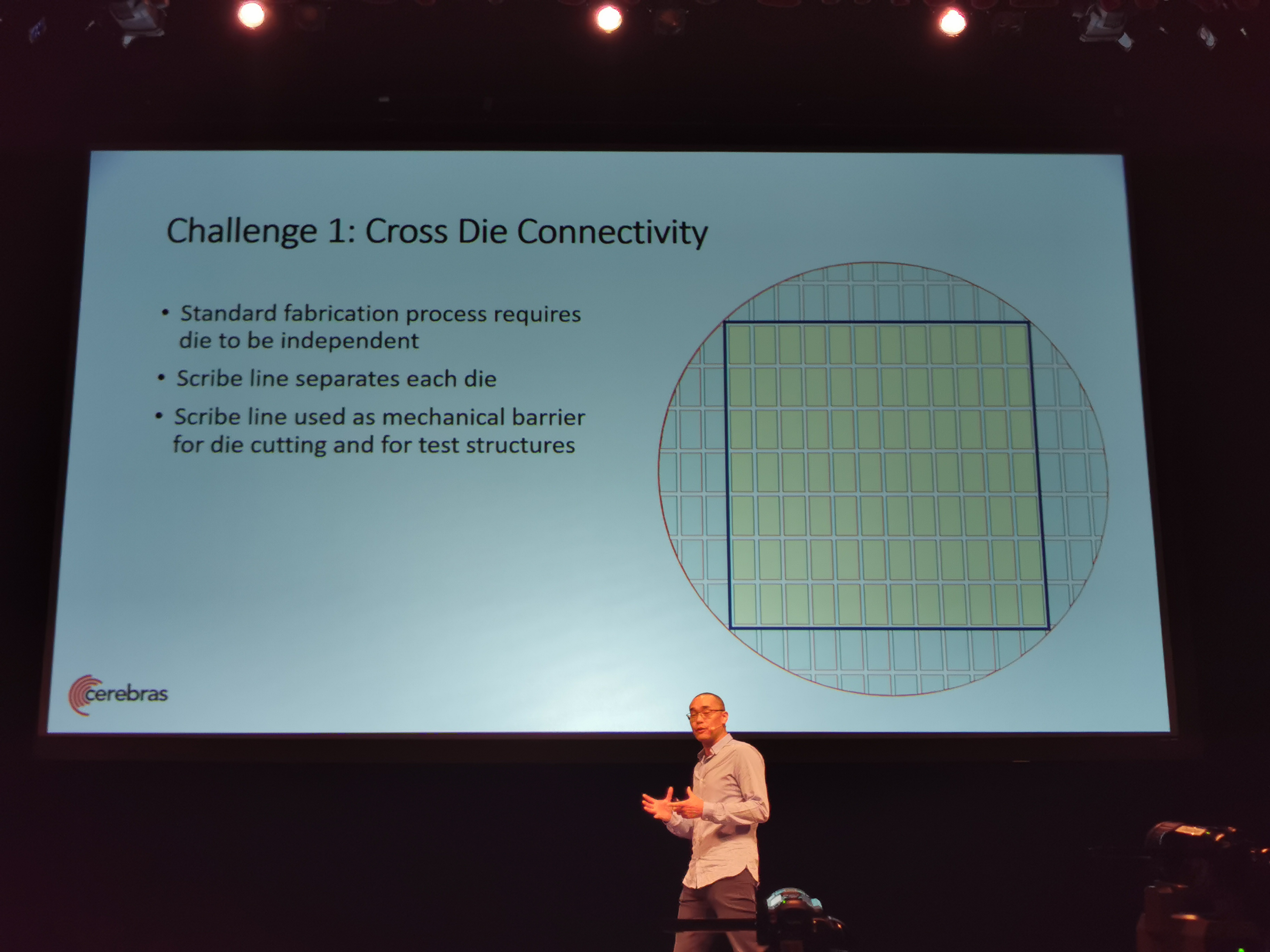
09:06PM EDT - Scribe line separates the die. On top of the scribe line, create wires
09:07PM EDT - Extends 2D mesh fabric across all die
09:07PM EDT - Same connectivity between cores and between die
09:07PM EDT - More efficient than off-chip
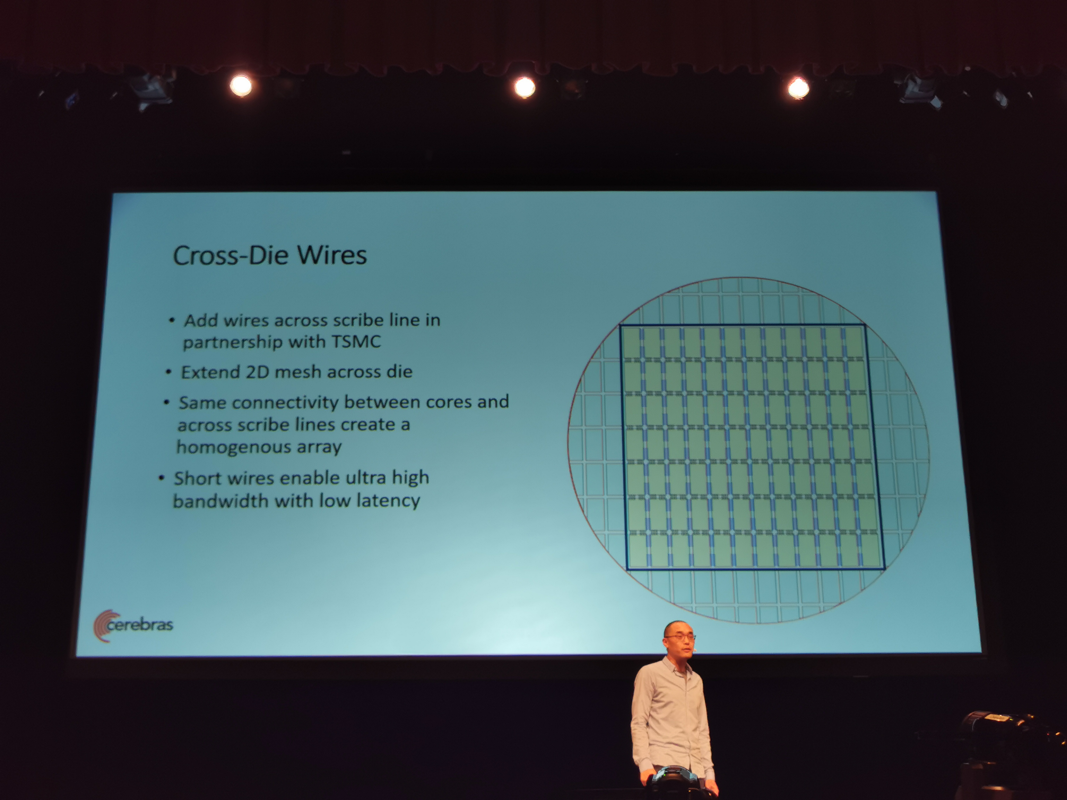
09:07PM EDT - Full BW at the die level
09:08PM EDT - Redundancy helps yield
09:08PM EDT - Redundant cores and redundant fabric links
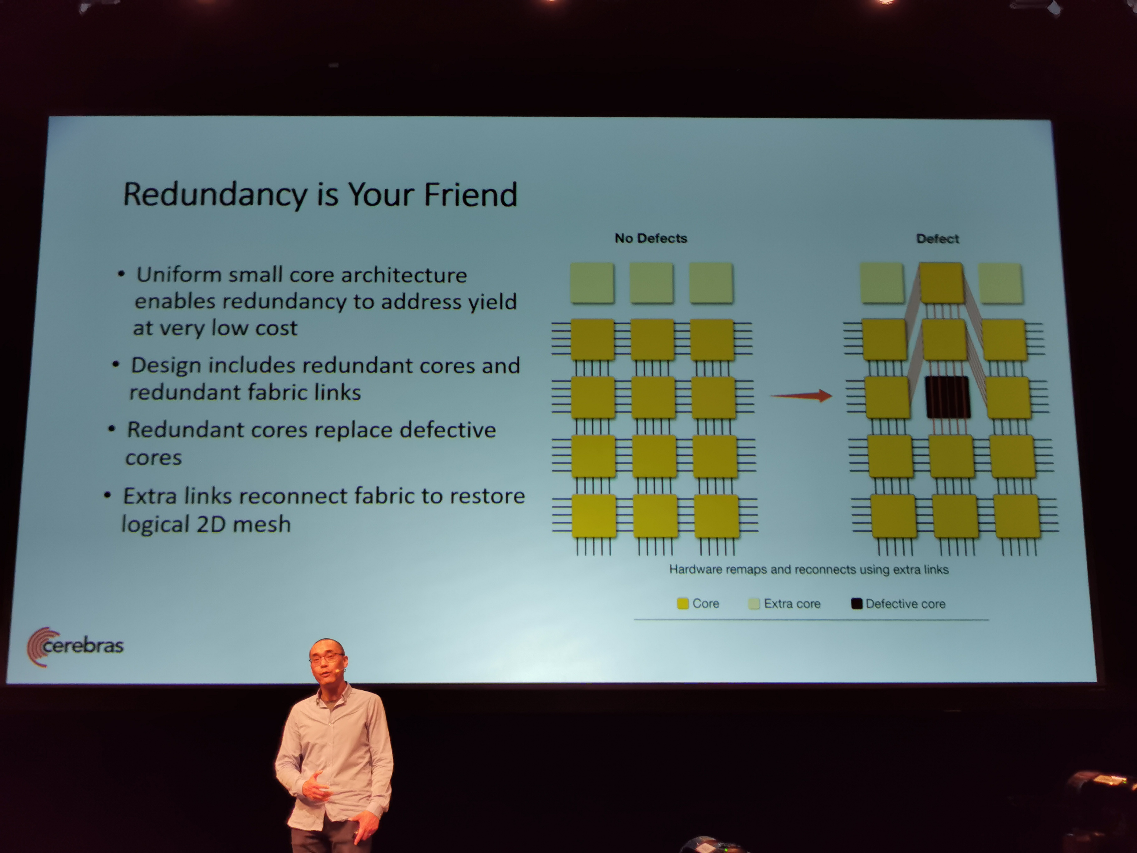
09:08PM EDT - Reconnect the fabric with links
09:08PM EDT - Drive yields high
09:09PM EDT - Transparent to software
09:09PM EDT - Thermal expansion
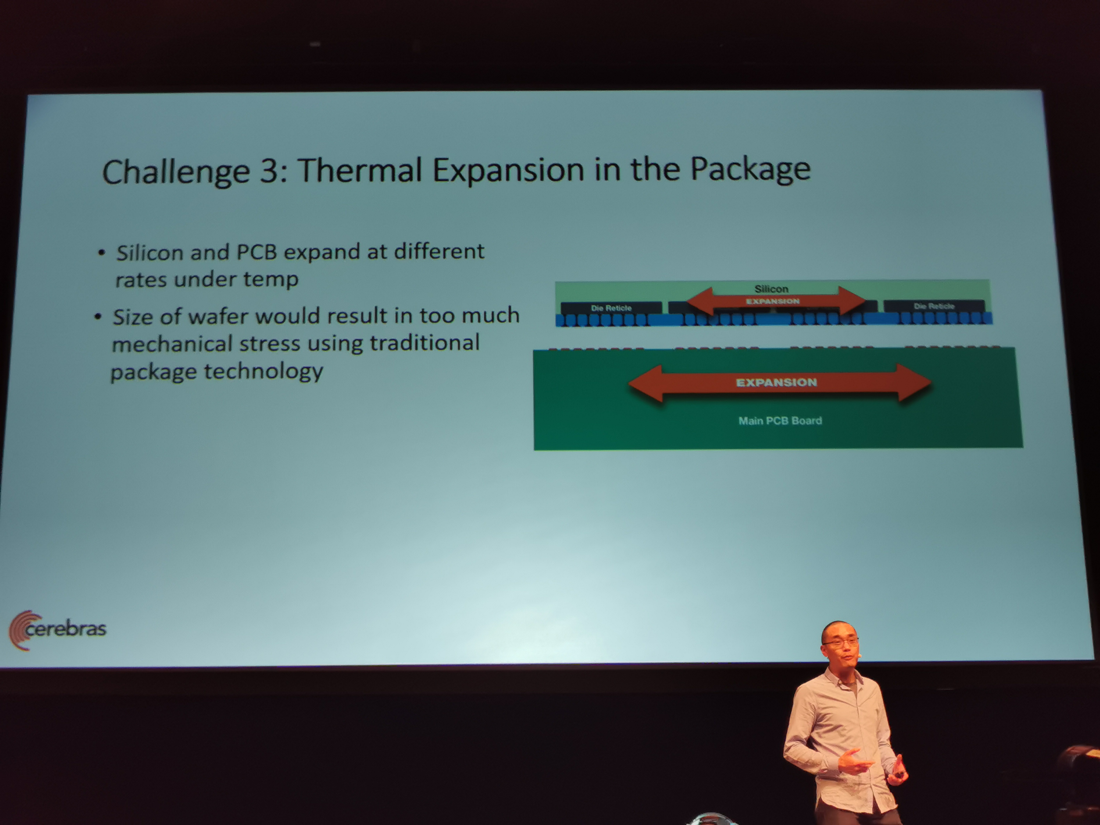
09:09PM EDT - Normal tech, too much mechanical stress via thermal expansion
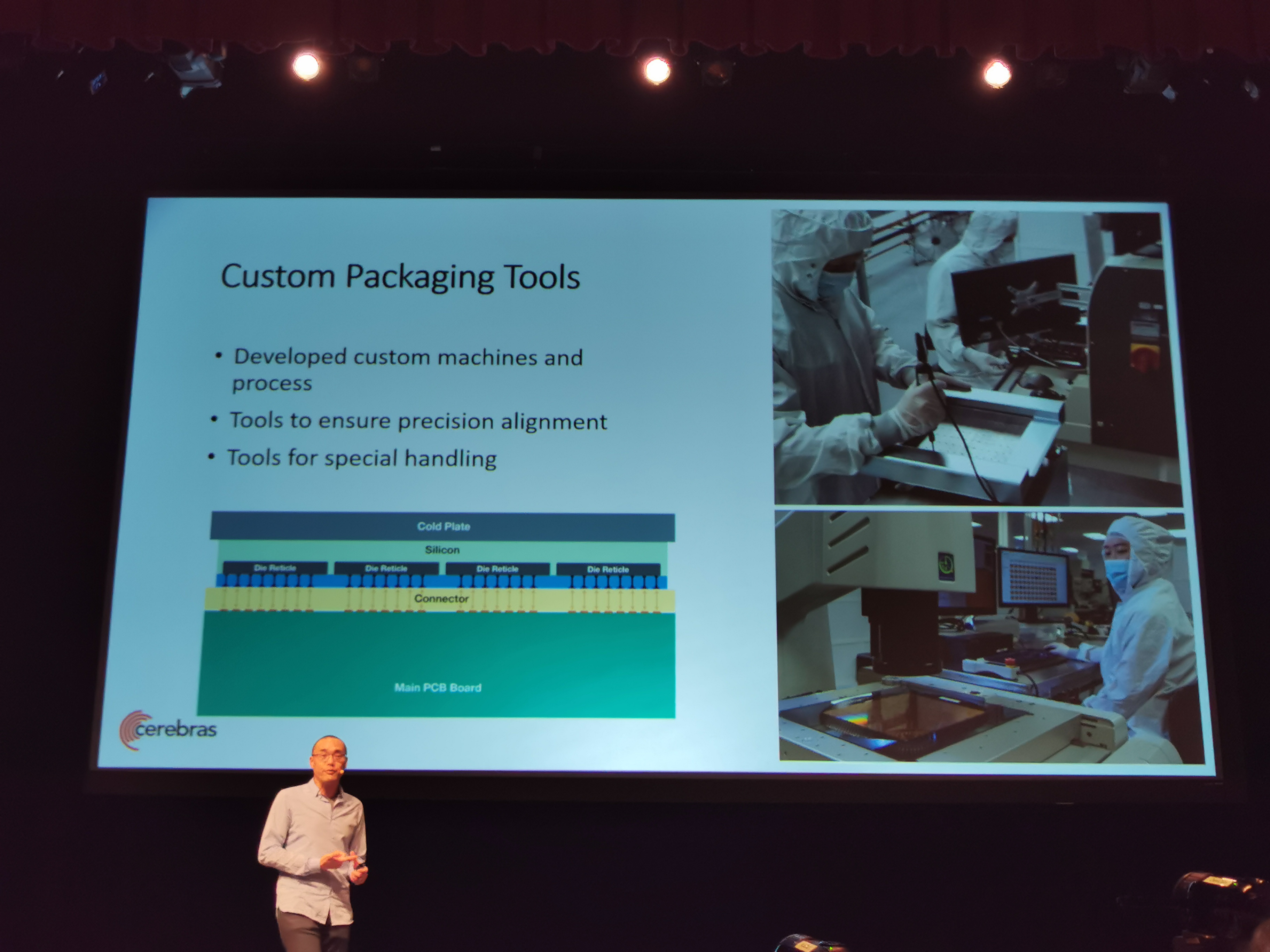
09:09PM EDT - Custom connector developed
09:09PM EDT - Connector absorbs the variation in thermal expansion
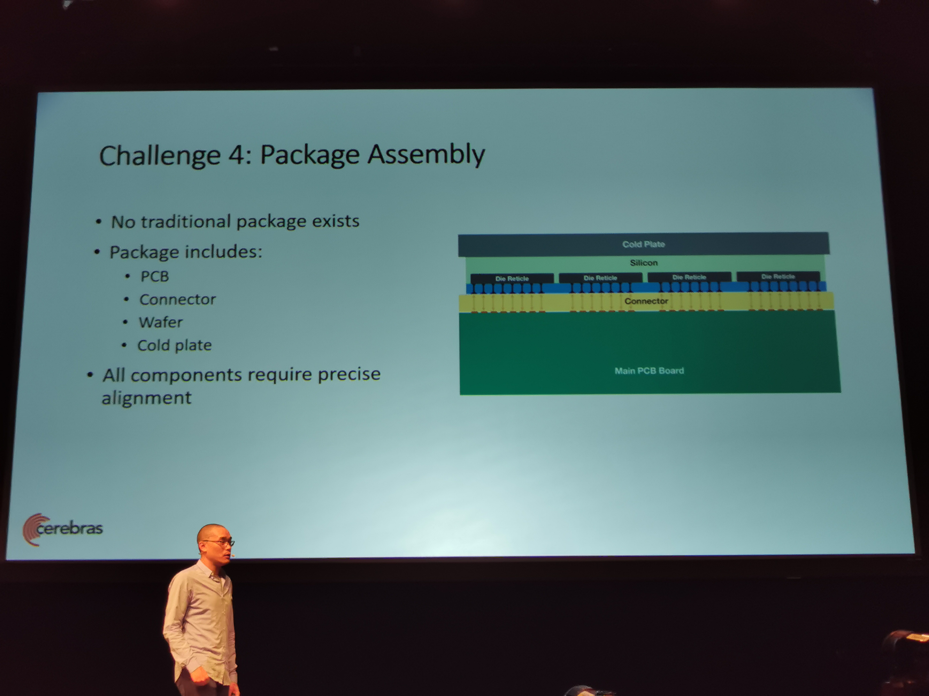
09:10PM EDT - All components need to be held with precise alignment - custom packaging tools
09:10PM EDT - Power and Cooling
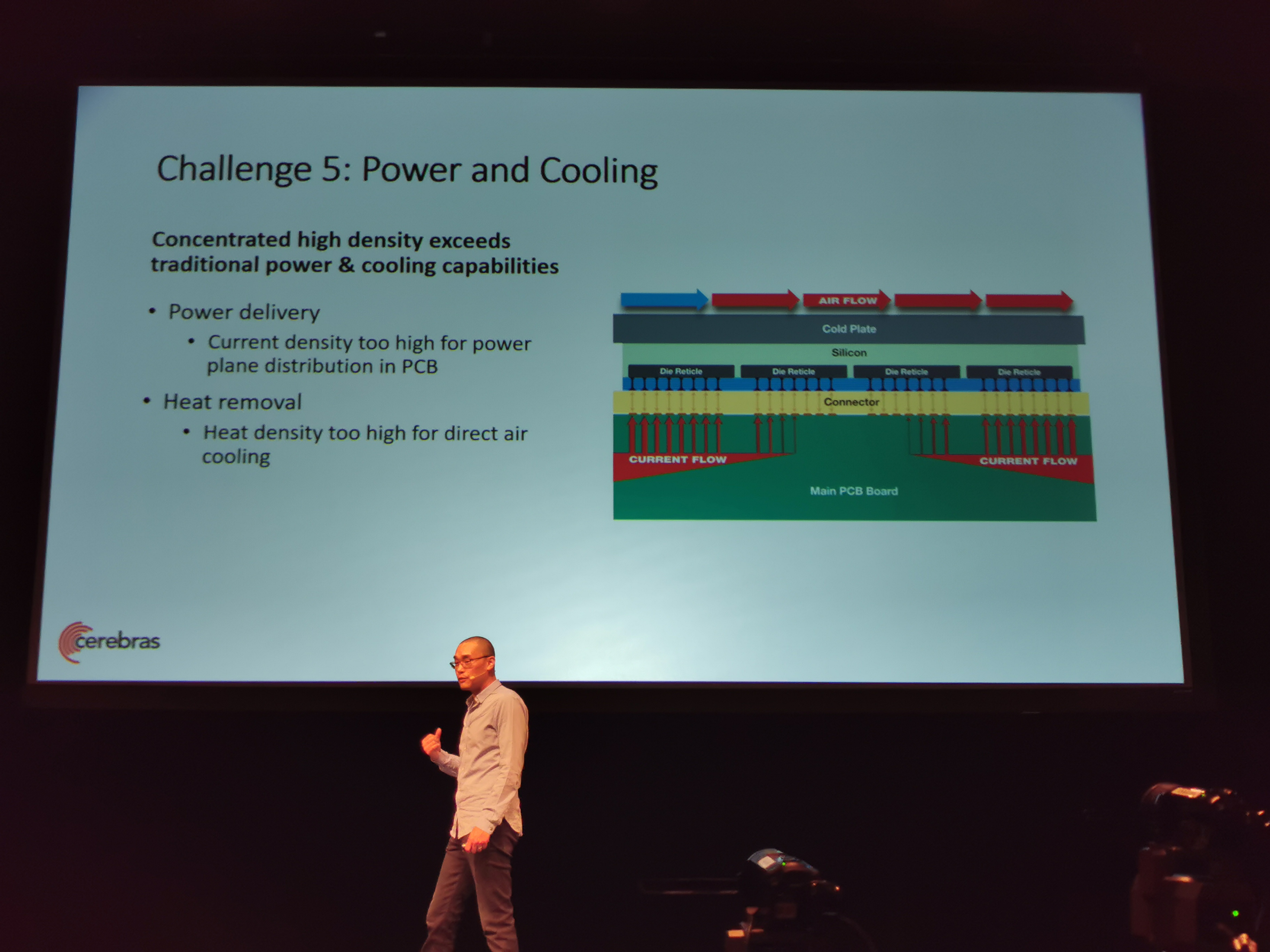
09:11PM EDT - Power planes don't work - isn't enough copper in the PCB to do it that way
09:11PM EDT - Heat density too high for direct air cooling
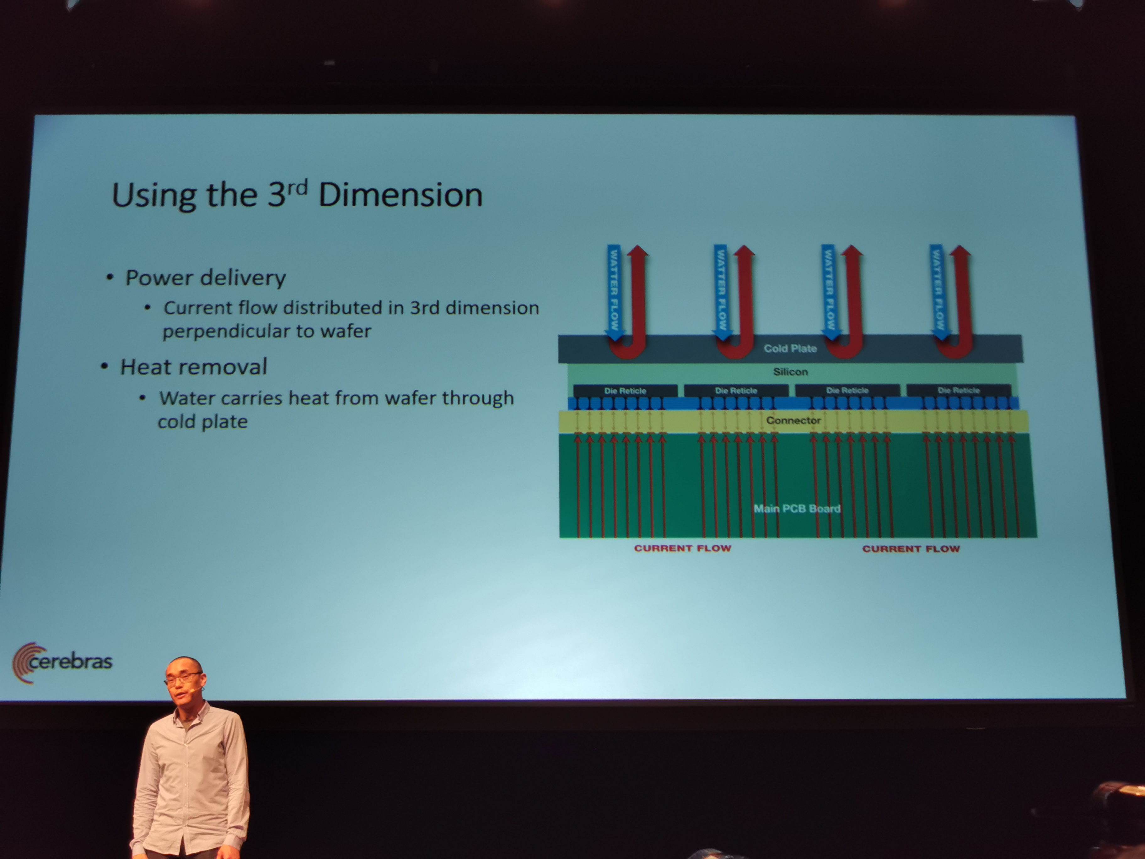
09:12PM EDT - Bring current perpendicular to the wafer. Water cooled perpendicular too
09:14PM EDT - Q&A Time

09:14PM EDT - Q and A
09:14PM EDT - Already in use? Yes
09:15PM EDT - Can you make a round chip? Square is more convenient
09:15PM EDT - Yield? Mature processes are quite good and uniform
09:16PM EDT - Does it cost less than a house? Everything is amortised across the wafer
09:17PM EDT - Regular processor for housekeeping? They can all do it
09:17PM EDT - Is it fully synchronous? No
09:20PM EDT - Clock rate? Not disclosed
09:20PM EDT - That's a wrap. Next is Habana


28 Comments
View All Comments
Andy Chow - Monday, August 19, 2019 - link
Incredible. I didn't believe it when I first saw an article about this. Because cross-die connectivity, which I know was something nVidia paid a lot for a larger overall individual die. But the full explanation makes sense. This is truly game-changing. I wonder about the clock rate. Is this 1+Ghz, or sub-200 Mhz?anonymous5 - Monday, August 19, 2019 - link
sub-200 Mhz probably would not even have thermal expansion or water cooling problems. has to be 1GHz+brakdoo - Tuesday, August 20, 2019 - link
You should have asked how this approach holds up against Panel-Level Packaging (PLP).Interconnect between chips would be slightly slower but all chips were 100% working, max possible size much bigger than these ~210x210mm, integration of DRAM/3DXPoint possible and everything would be much cheaper.
Duncan Macdonald - Tuesday, August 20, 2019 - link
Is the faulty core bypass fixed or changeable (ie if a core fails sometime in the future can it be bypassed) ?How are defective inter die links handled ?
Ian Cutress - Friday, August 23, 2019 - link
It looks like there are about 1-1.5% spare cores onboard, and defective cores are bypassed with one of the spare cores being enabled in its place.Achtung_BG - Tuesday, August 20, 2019 - link
46225 mm2 OMG!!! One chip per wafer unbelievable....PixyMisa - Tuesday, August 20, 2019 - link
I anticipate a moderate degree of expense in acquiring this device.PeachNCream - Wednesday, August 21, 2019 - link
And the understatement of the year award goes to PixyMisa!willis936 - Tuesday, August 20, 2019 - link
The Q to A ratio in that Q and A session is quite low.eastcoast_pete - Tuesday, August 20, 2019 - link
Thanks Ian! Amazing chip, but my question is (would have been if there): How fault-tolerant is this design? We all know that as the transistor count goes up, so does the chance of having too many manufacturing defects that render an IC useless. With this enormous number of transistors, the accumulated number of faults must be substantial. I know they addressed fault-tolerance, but only sort-of. Do they have a (even just one) functional chip they can demonstrate? Showing silicon but not silicon in action raises more questions for me than it answers.