Intel Announces The FPGA PAC N3000 for 5G Networks
by Andrei Frumusanu on March 4, 2019 3:00 PM EST- Posted in
- MWC 2019
- Networking
- Intel
- Infrastructure
- FPGA PAC N3000
One of last week’s early MWC 2019 announcements was Intel’s new FPGA PAC N3000 card. Intel’s networking business is something that the company has been focusing a lot of the last couple of years as it offers some interesting opportunities both to Intel as a supplier as well as to potential customers.
Intel’s new PAC solution represents a new tier among the company’s portfolio, aimed directly at telecom providers who have to deal with ever increasing data traffic. In particular Intel is marketing the need for such specialised (yet flexible) solutions to be able to cope with the transition to 5G.

Traditional solutions would have to rely either on software solutions, which many times is either too slow an inflexible, or on dedicated silicon hardware, which has high investment cost and a long lead time in terms of implementation. The new FPGA PAC N3000 aims at combining the benefits of both worlds, achieving much higher throughput than would be possible by software acceleration, all while being flexible enough for customers to deploy it easily and fast.

At the heart of the new card we find an Arria 10 GT1150 FPGA chip with 1.15 million logic elements, representing the tier SKU in Intel’s Arria lineup.
The memory configuration of the new PAC N3000 seems odd at first, as it’s listed at 9GB of DDR4. In fact what we’re dealing with here is a three-tier DRAM subsystem: the card has 8GB of 64-bit DDR4, 1GB of 16-bit DDR4 as well as 144MB of QDR IV memory. The rationale here is that the different memory hierarchies serve different workloads running on the card, with different tasks having their own optimised memory tiers, taking full advantage of various bandwidth and latency characteristics. Intel for example explains that the 1GB of 16-bit DDR4 represents a lower latency memory buffer than the full 8GB buffer, and the 144MB QDR buffer is even further latency optimised and specifically serves tasks such as hosting the QoS tables of the software stack.
Network connectivity is provided by two Intel Converged Network Adapter XL710’s which are integrated into the card, serviced by two QSFP connectors. This enables connectivity up to 100Gbps in either 8x10 or 4x25Gbps configurations.
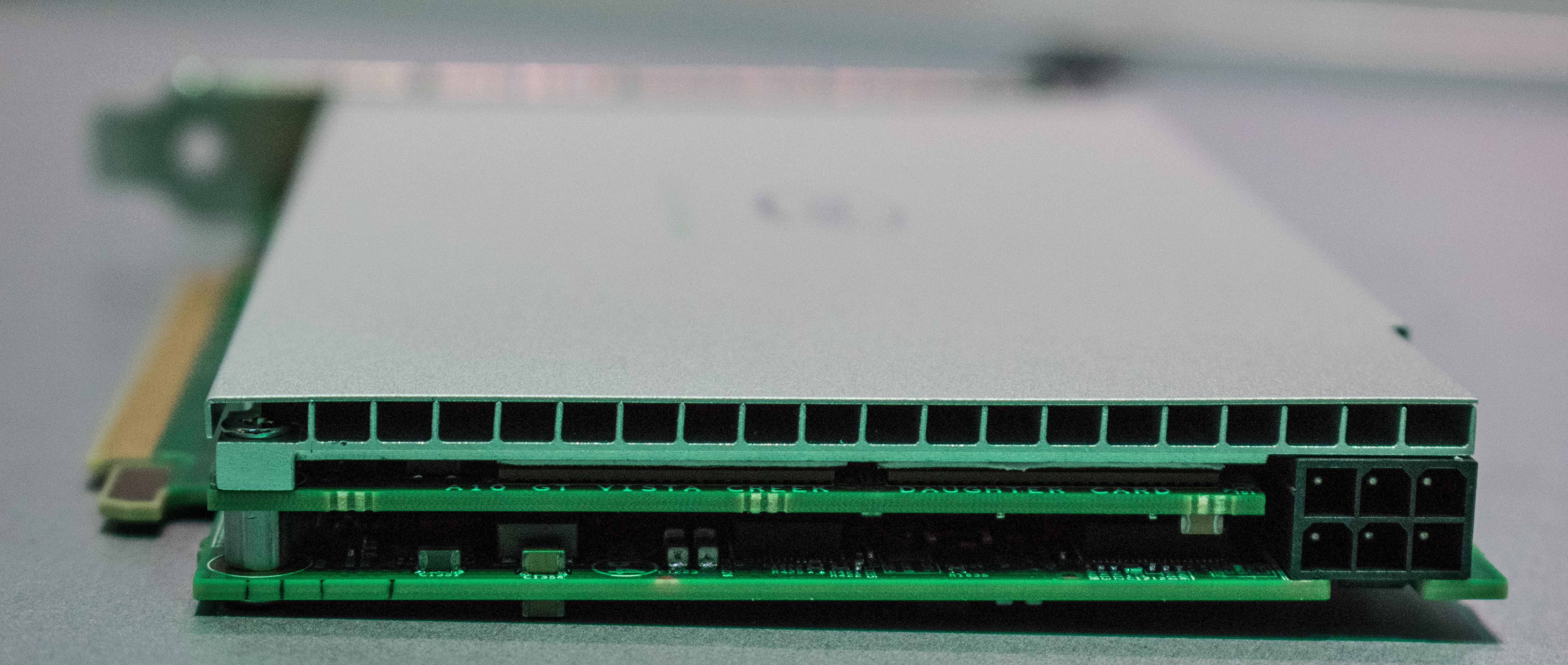
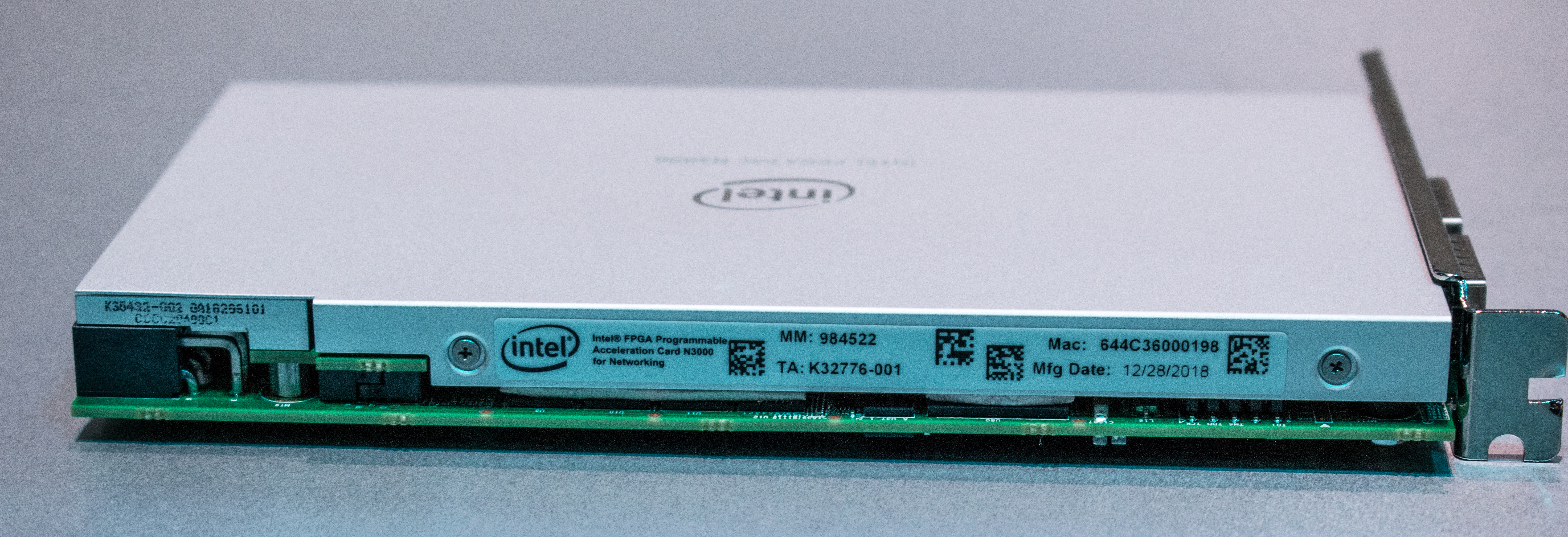
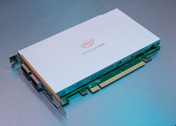
We were able to get our hands on the card at Intel’s MWC 2019 booth, showcasing more details: The card is a single-slot, half-length board with a PCIe 3.0 x16 connector.
What is interesting is that the board itself is actually a multi-PCB design – unfortunately Intel wouldn’t let us remove the heat-sink or detail the innards, but it’s easy to envision that the upper PCB layer hosts the XL710 network card components while the main board is hosting the FPGA.
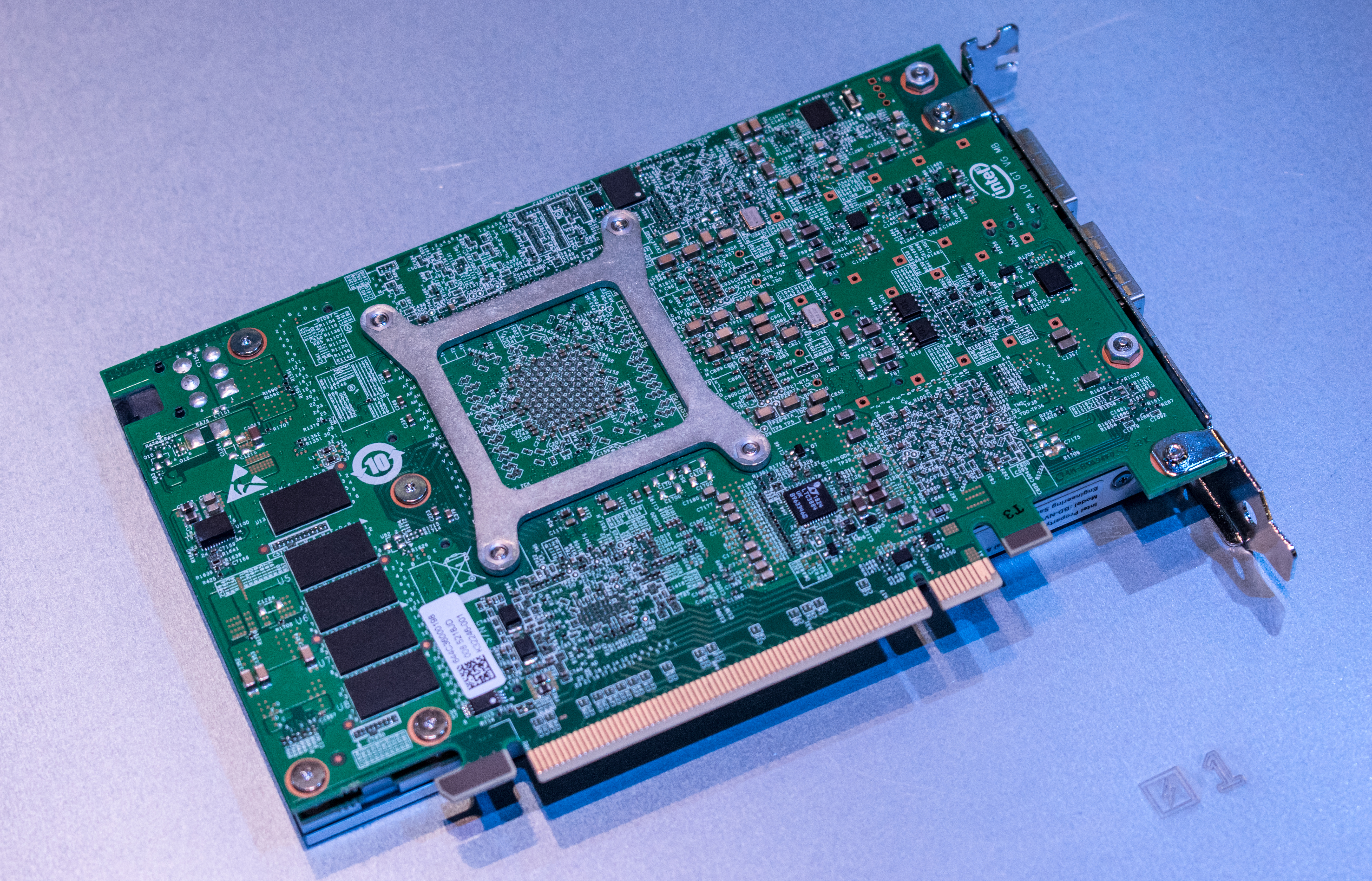
The back of the card looks eerily similar to a graphics card, and we can note Micron DDR4 chips arranged in a 4+1 configuration (64+16-bit channels).

Intel’s goal with the card is to offer network operators with a quick solution to their 5G network needs, offering a time and flexibility advantage over competing (possibly more integrated) solutions.
Related Reading:


2 Comments
View All Comments
The Chill Blueberry - Monday, March 4, 2019 - link
Looks meaty with the stacked PCBs and all those SMDs!brakdoo - Monday, March 4, 2019 - link
The QDR memory is not "further latency optimized", it's SRAM with low latency in any case...