AMD Unveils ‘Chiplet’ Design Approach: 7nm Zen 2 Cores Meet 14 nm I/O Die
by Anton Shilov on November 6, 2018 1:53 PM EST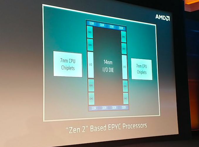
AMD on Tuesday disclosed some additional details about its upcoming codenamed Rome processor based on its Zen 2 microarchitecture. As it turns out, the company will use a new design approach with its next-generation EPYC CPUs that will involve CPU ‘chiplets’ made using TSMC’s 7 nm manufacturing technology as well as an I/O die made using a 14 nm fabrication process.
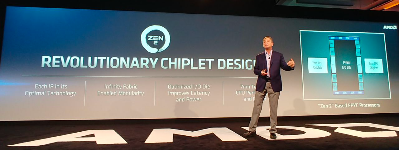
AMD’s chiplet design approach is an evolution of the company’s modular design it introduced with the original EPYC processors featuring its Zen microarchitecture. While the currently available processors use up to four Zen CPU modules, the upcoming EPYC chips will include multiple Zen 2 CPU modules (which AMD now calls ‘chiplets’) as well as an I/O die made using a mature 14 nm process technology. The I/O die will feature Infinity Fabrics to connect chiplets as well as eight DDR DRAM interfaces. Since the memory controller will now be located inside the I/O die, all CPU chiplets will have a more equal memory access latency than today’s CPU modules. Meanwhile, AMD does not list PCIe inside the I/O die, so each CPU chiplet will have its own PCIe lanes.
Separating CPU chiplets from the I/O die has its advantages because it enables AMD to make the CPU chiplets smaller as physical interfaces (such as DRAM and Infinity Fabric) do not scale that well with shrinks of process technology. Therefore, instead of making CPU chiplets bigger and more expensive to manufacture, AMD decided to incorporate DRAM and some other I/O into a separate chip. Besides lower costs, the added benefit that AMD is going to enjoy with its 7 nm chiplets is ability to easier bin new chips for needed clocks and power, which is something that is hard to estimate in case of servers.
This is a breaking news. We are updating the news story with more details.
Source: AMD


76 Comments
View All Comments
iwod - Tuesday, November 6, 2018 - link
It is interesting we have come a full circle, when DDR used to be in "Chipset", we then moved the memory controller to the CPU now we are back again.ravyne - Tuesday, November 6, 2018 - link
Kind of. Its still in the CPU socket, so the bus width can be a lot larger and lower latency than olden-style northbridges could ever dream of. The advantages of on-die memory controllers can start to be swamped when those dies start needing to communicate with each other to access non-local memory and IO.Ideas don't always fade to history, sometimes echos of an old idea make sense again in light of other engineering decisions made in modern times. Back when memory controllers moved on-die, it made sense because off-chip controllers were a bottle-neck. Now, the scalability of IO interfaces eats die-area that could be better spent on compute.
mapesdhs - Tuesday, November 6, 2018 - link
I see echoes of SGI's old Crossbar chip:http://www.sgidepot.co.uk/chipsdiagram.gif
As Mashey used to say, it's all about the bandwidth. 8)
Alexvrb - Tuesday, November 6, 2018 - link
El blasto from el pasto.lefty2 - Wednesday, November 7, 2018 - link
Most software is NUMA aware, so there is very little non-local memory access in realityNICK1358 - Tuesday, November 13, 2018 - link
And what about compatibility with "older" chipsets as x470? will it support the new processors?PeachNCream - Tuesday, November 6, 2018 - link
The Infinity Fabric...doesn't it already account for a healthy chunk of the total power consumption of Zen-based products? Leaving it on a 14nm node and migrating the memory interface to it while putting the CPUs on 7nm may further increase the ratio of power consumed by the non-CPU portion of the processor package. I get that the decision is probably made in light of a lot of factors beyond just power consumption, but it looks like we're losing some efficiency gains offered by newer and smaller nodes and that speaks to how much closer we've gotten to the physical limits of the materials we currently use to produce processors.Alistair - Tuesday, November 6, 2018 - link
article:physical interfaces (such as DRAM and Infinity Fabric) do not scale that well with shrinks of process technology
PeachNCream - Tuesday, November 6, 2018 - link
Scaling could mean other things besides just a reduction in power. I read that as a possible problem with reaching good yields (say throwing out a die with good CPUs because of a faulty DRAM controller or some problem with the IF - which might explain why recently released TR2s have only two dies with DRAM controllers enabled as the other two could be defective parts) or ramping up IF and DRAM controller clock speed. Power is, of course, a concern as well in the scaling discussion but we lack enough information in the article to, with such certainty, rule out other factors.SleepyFE - Wednesday, November 7, 2018 - link
When you scale things down you use less space and send less electrons through. That's how you get power savings. When sending signals through a comm line you have to be careful about crosstalk. So you either can't send more electrons (that would ensure a good read), or you need to space the comm lines more (even if they are smaller) negating the node shrink. With newer SSD controllers the QLC needs to read 16 voltage states, so it needs to be able to tell apart very small differences in voltage. The controller also has a lot more power (compared to older ones) and can use better error correction. Error correction in a CPU would take up compute resources.In conclusion: If it works, don't break it.