Samsung Foundry

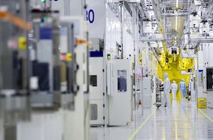
As part of Samsung's Q1 earnings announcement, the company has outlined some of its foundry unit's key plans for the rest of the year. The company has confirmed that it remains on track to meeting its goal of starting mass production of chips on its SF3 (3 nm-class, 2nd Generation) technology in the second half of the year. Meanwhile in June, Samsung Foundry will formally unveil its SF2 (2 nm-class) process technology, which will offer a mix of performance and efficiency enhancements. Finally, the company the company is preparing a variation of its 4 nm-class technology for integration into stacked 3D designs. SF2 To Be Unveiled In June Samsung plans to disclose key details about its SF2 fabrication technology at the VLSI Symposium 2024 on June...
IBM to use Samsung 7nm EUV for Next-Gen POWER and z CPUs
IBM has announced it has signed an agreement with Samsung Foundry to produce its next-generation processors. This includes processors for IBM Power Systems, IBM z, and LinuxONE systems, all...
24 by Anton Shilov on 12/21/2018
Samsung Starts Mass Production of Chips Using Its 7nm EUV Process Tech
Samsung Foundry on Wednesday said that it had started production of chips using its 7LPP manufacturing technology that uses extreme ultraviolet lithography (EUVL) for select layers. The new fabrication...
42 by Billy Tallis & Anton Shilov on 10/17/2018
Samsung Foundry Updates: 8LPU Added, EUVL on Track for HVM in 2019
Samsung recently hosted its Samsung Foundry Forum 2018 in Japan, where it made several significant foundry announcements. Besides reiterating plans to start high-volume manufacturing (HVM) using extreme ultraviolet lithography...
29 by Anton Shilov on 9/6/2018
Arm and Samsung Extend Artisan POP IP Collaboration to 7LPP and 5LPE Nodes
Arm and Samsung Foundry this week announced plans to extend their collaboration to 7LPP and 5LPE process technologies. Under the terms of the agreement, Arm will offer Samsung Foundry...
23 by Anton Shilov on 7/6/2018
Samsung to Pay $400 Million for Infringing FinFET Patent
A federal jury in Texas ordered Samsung Electronics to pay $400 million to a South Korean university for infringing one of fundamental patents related to double gate FinFET transistors...
33 by Anton Shilov on 6/19/2018
Samsung Foundry Roadmap: EUV-Based 7LPP for 2018, 3 nm Incoming
Samsung Foundry this week updated its fabrication technology roadmap, introducing a number of changes and announcing the first details about its 3 nm manufacturing process that is several years...
25 by Anton Shilov on 5/24/2018
Samsung Starts Mass Production of Chips Using 10nm Low Power Plus (10LPP) Process Tech
Samsung Foundry on Wednesday revealed that it has started mass production of SoC products using its second generation 10 nm Low Power Plus (10LPP) fabrication technology. The new manufacturing...
10 by Anton Shilov on 11/29/2017


