N5
Taiwan Semiconductor Manufacturing Co. this week said its revenue for the second quarter 2024 reached $20.82 billion, making it the company's best quarter (at least in dollars) to date. TSMC's high-performance computing (HPC) platform revenue share exceeded 52% for the first time in many years due to demand for AI processors and rebound of the PC market. TSMC earned $20.82 billion USD in revenue for the second quarter of 2024, a 32.8% year-over-year increase and a 10.3% increase from the previous quarter. Perhaps more remarkable, $20.82 billion is a higher result than the company posted Q3 2022 ($20.23 billion), the foundry's best quarter to date. Otherwise, in terms of profitability, TSMC booked $7.59 billion in net income for the quarter, for a gross margin of...
TSMC Posts Q1'24 Results: 3nm Revenue Share Drops Steeply, but HPC Share Rises
Taiwan Semiconductor Manufacturing Co. this week released its financial results for Q1 2024. Due to a rebound in demand for semiconductors, the company garned $18.87 billion in revenue for...
11 by Anton Shilov on 4/19/2024
TSMC Delays Arizona Fab Deployment to 2025, Citing Shortage of Skilled Workers
TSMC on Thursday disclosed that it will have to delay mass production at its Fab 21 in Arizona to 2025, as a lack of suitably skilled workers is slowing...
27 by Anton Shilov on 7/20/2023
TSMC Details N4X Process for HPC: Extreme Performance at Minimum Leakage
At its 2023 Technology Symposium TSMC revealed some additional details about its upcoming N4X technology that is designed specifically for high-performance computing (HPC) applications. This node promises to enable...
5 by Anton Shilov on 5/26/2023
TSMC Unveils Major U.S. Fab Expansion Plans: 3nm and $40 Billion by 2026
TSMC this week held its Arizona fab 'first tool-in' ceremony, where alongside celebrating its first US fab, the company also announced major expansion plans for the production facility. The...
17 by Anton Shilov on 12/7/2022
TSMC and ASML: Demand for Chips Remains Strong, But Getting Fab Tools Is Hard
TSMC's revenue this year is going to set an all-time record for the company, thanks to high demand for chips as well as increased prices that its customers are...
13 by Anton Shilov on 7/21/2022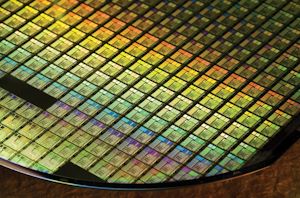
TSMC Unveils N4X Node: Extreme High-Performance at High Voltages
TSMC this week announced a new fabrication process that is tailored specifically for high-performance computing (HPC) products. N4X promises to combine transistor density and design rules of TSMC's N5-family...
42 by Anton Shilov on 12/17/2021
AMD Gives Details on EPYC Zen4: Genoa and Bergamo, up to 96 and 128 Cores
Since AMD’s relaunch into high-performance x86 processor design, one of the fundamental targets for the company was to be a competitive force in the data center. By having a...
36 by Dr. Ian Cutress on 11/8/2021
An AnandTech Interview with TSMC: Dr. Kevin Zhang and Dr. Maria Marced
In the past week, TSMC ran its 2021 Technology Symposium, covering its latest developments in process node technology designed to improve the performance, costs, and capabilities for its customers...
18 by Dr. Ian Cutress on 6/8/2021
TSMC Manufacturing Update: N6 to Match N7 Output by EOY, N5 Ramping Faster, Better Yields Than N7
As part of a regular TSMC Technology Symposium, the foundry published updates on its status on it’s current leading-edge manufacturing technologies, the N7, N5 and their respective derivatives such...
50 by Andrei Frumusanu on 6/1/2021
TSMC Update: 2nm in Development, 3nm and 4nm on Track for 2022
For TSMC, being the world's largest foundry with nearly 500 customers has its peculiarities. On the one hand, the company can serve almost any client with almost any requirements...
74 by Anton Shilov on 4/26/2021
TSMC to Spend $100B on Fabs and R&D Over Next Three Years: 2nm, Arizona Fab & More
TSMC this week has announced plans to spend $100 billion on new production facilities as well as R&D over the next three years. The world's largest contract maker of...
45 by Anton Shilov on 4/2/2021Marvell Announces 112G SerDes, Built on TSMC 5nm
So far we have three products in the market built on TSMC’s N5 process: the Huawei Kirin 9000 5G SoC, found in the Mate 40 Pro, the Apple A14...
15 by Dr. Ian Cutress on 11/17/2020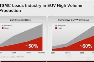
TSMC: We have 50% of All EUV Installations, 60% Wafer Capacity
One of the overriding central messages to TSMC’s Technology Symposium this week is that the company is a world leader in semiconductor manufacturing, especially at the leading edge process...
32 by Dr. Ian Cutress on 8/27/2020
TSMC Expects 5nm to be 11% of 2020 Wafer Production (sub 16nm)
One of the measures of how quickly a new process node gains traction is by comparing how many wafers are in production, especially as that new process node goes...
13 by Dr. Ian Cutress on 8/25/2020
‘Better Yield on 5nm than 7nm’: TSMC Update on Defect Rates for N5
One of the key metrics on how well a semiconductor process is developing is looking at its quantitative chip yield – or rather, its defect density. A manufacturing process...
107 by Dr. Ian Cutress on 8/25/2020
TSMC Details 3nm Process Technology: Full Node Scaling for 2H22 Volume Production
At TSMC’s annual Technology Symposium, the Taiwanese semiconductor manufacturer detailed characteristics of its future 3nm process node as well as laying out a roadmap for 5nm successors in the...
58 by Andrei Frumusanu on 8/24/2020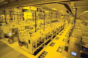
TSMC & Broadcom Develop 1,700 mm2 CoWoS Interposer: 2X Larger Than Reticles
With transistor shrinks slowing and demand for HPC gear growing, as of late there has been an increased interest in chip solutions larger than the reticle size of a...
18 by Anton Shilov on 3/4/2020
TSMC Boosts CapEx by $1 Billion, Expects N5 Node to Be Major Success
TSMC is on track to begin high-volume production of chips using its 5 nm technology in the coming months, the company said in its conference call last week. While...
40 by Anton Shilov on 1/22/2020
TSMC: 5nm on Track for Q2 2020 HVM, Will Ramp Faster Than 7nm
TSMC’s 5 nm (N5) manufacturing technology is projected to provide significant benefits when it comes to performance, power, and area scaling, which is why the contract maker of semiconductors...
27 by Anton Shilov on 10/23/2019


