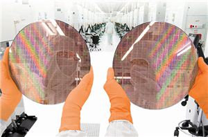
14LPP
Despite most discussion about chip manufacturing focusing on the leading edge and blazingly fast and complex side of the industry, the demand for the ‘legacy’ process technologies is also higher than ever, but also by volume a lot bigger than the latest and greatest. These legacy processes form the backbone of most modern electronics, and so being able to offer equivalent technology at lower cost/power is often a win-win for manufacturers and chip designers alike. To that end, Samsung is announcing a new 17nm process node, designed for customers still using a planar 28nm process, but want to take advantage of 14nm FinFET technology.
GlobalFoundries Unveils 12LP+ Technology: Massive Performance & Power Improvements
GlobalFoundries has introduced its 12LP+ fabrication process that relies on the groundwork set by its 14LPP and 12LP technologies and provides significant improvements when it comes to performance, power...
41 by Anton Shilov on 9/25/2019GlobalFoundries Establishes Avera Semiconductor: a Custom Chip Company
GlobalFoundries this week announced that it has spun off its ASIC Solutions division, establishing Avera Semiconductor, a wholly owned subsidiary that will help fabless chip developers to design their...
11 by Anton Shilov on 11/2/2018GlobalFoundries Adds 12LP Process for Mainstream and Automotive Chips; AMD Planning 12LP CPUs & GPUs
GlobalFoundries on Wednesday announced its new 12LP (leading performance) fabrication process. The new manufacturing technology was designed to increase transistor density and improve frequency potential compared to GlobalFoundries’ current-gen...
32 by Anton Shilov on 9/21/2017Samsung Announces Second-Gen 14nm Low Power Plus (14LPP) Process Now In Mass Production
Today Samsung Semiconductor officialy announces mass production for its second generation 14nm FinFET manufacturing node. Early last year we saw Samsung announce mass production of its first generation FinFET...
32 by Andrei Frumusanu on 1/14/2016


