Skylake Iris Pro hits Intel’s Pricing Lists: Xeon E3-1575M v5 with GT4e
by Ian Cutress on January 26, 2016 12:17 PM EST- Posted in
- CPUs
- Intel
- Mobile Workstation
- Xeon
- Mobile
- Laptops
- Enterprise
- Skylake
- eDRAM

One of our forum members, Sweepr, posted Intel’s latest pricing list for OEMs dated the 24th of January and it contained a number of interesting parts worth documenting. The Braswell parts and Skylake Celerons were disclosed over the past few months are now available to OEMs, but it’s the parts with Iris Pro that have our attention.
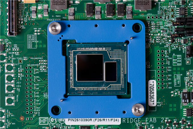
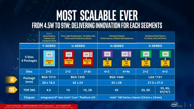
Iris Pro is Intel’s name for their high end graphics solution. Using their latest graphics microarchitecture, Gen9, Iris Pro packs in the most execution units (72) as well as a big scoop of eDRAM. At the minute we assume it’s the 128 MB edition as Intel’s roadmaps have stated a 4+4e part only on mobile, rather than a 4+3e part with 64 MB (only the 2+3e parts are listed as 64MB), although we are looking for confirmation.
The new parts are listed as:
Xeon E3-1575M v5 (8M cache, 4 Cores, 8 Threads, 3.00 GHz, 14nm) - $1,207
Xeon E3-1545M v5 (8M cache, 4 Cores, 8 Threads, 2.90 GHz, 14nm) - $679
Xeon E3-1515M v5 (8M cache, 4 Cores, 8 Threads, 2.80 GHz, 14nm) - $489
These will compare to the non-Iris Pro counterparts, running P530 graphics (4+2, 24 EUs):
Xeon E3-1535M v5 (8M cache, 4 Cores, 8 Threads, 2.90 GHz, 14nm) - $623
Xeon E3-1505M v5 (8M cache, 4 Cores, 8 Threads, 2.80 GHz, 14nm) - $434
As Sweepr points out, the difference between the 2.8-2.9 GHz parts is only $55-56. That is for both the increase in graphics EUs (24 to 72) as well as that extra on-package eDRAM.

The i7-4950HQ with 128 MB eDRAM
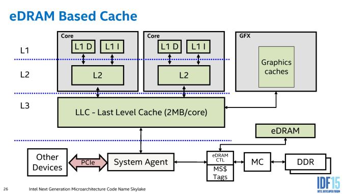
We have more reasons to be excited over the eDRAM in Skylake than what we saw before in Haswell with the i7-4950HQ on mobile and Broadwell on desktop with the i7-5775C, i5-5765C and the relevant Xeons. With the older platforms, the eDRAM was not a proper bidirectional cache per se. It was used as a victim cache, such that data that was spurned from the L3 cache on the CPU ended up in eDRAM, but the CPU could not place data from the DRAM into the eDRAM without using it first (prefetch prediction). This also meant that the eDRAM was invisible to any other devices on the system, and without specific hooks couldn’t be used by most software or peripherals.
With Skylake, this changes, the eDRAM lies beyond the L3 and the System Agent as a pathway to DRAM, meaning that any data that wants DRAM space will go through the eDRAM in search for it. Rather than acting as a pseudo-L4 cache, the eDRAM becomes a DRAM buffer and automatically transparent to any software (CPU or IGP) that requires DRAM access. As a result, other hardware that communicates through the system agent (such as PCIe devices or data from the chipset) and requires information in DRAM does not need to navigate through the L3 cache on the processor. Technically graphics workloads still need to circle around the system agent, perhaps drawing a little more power, but GPU drivers need not worry about the size of the eDRAM when it becomes buffer-esque and is accessed before the memory controller is adjusted into a higher power read request. The underlying message is that the eDRAM is now observed by all DRAM accesses, allowing it to be fully coherent and no need for it to be flushed to maintain that coherence. Also, for display engine tasks, it can bypass the L3 when required in a standard DRAM access scenario. While the purpose of the eDRAM is to be as seamless as possible, Intel is allowing some level on control at the driver level allowing textures larger than the L3 to reside only in eDRAM in order to prevent overwriting the data contained in the L3 and having to recache it for other workloads.
We go into more detail on the changes to Skylake’s eDRAM in our microarchitecture analysis piece, back from September.
The fact that Intel is approaching the mobile Xeon market first, rather than the consumer market as in Haswell, should be noted. eDRAM has always been seen as a power play for heavy DRAM workloads, which arguably occur more in professional environments. That still doesn’t stop desktop users requesting it as well – the fact that the jump from 4+2 to a 4+4e package is only $55-$56 means that if we apply the same metrics to desktop processors, an i5-6600K with eDRAM would be $299 in retail (vs. $243 MSRP on the standard i5-6600K).
One of the big tasks this year will be to see how the eDRAM, in the new guise as a DRAM buffer, makes a difference to consumer and enterprise workloads. Now that there are two pairs of CPUs on Intel’s pricing list that are identical aside from the eDRAM, we have to go searching for a source. It seems that HP has already released a datasheet showing the HP ZBook 17 G3 Mobile Workstation as being offered with the E3-1575 v5, which Intel lists as a whopping $1207. That's certainly not the extra $55.
Source: AnandTech Forums, Intel


72 Comments
View All Comments
BurntMyBacon - Thursday, January 28, 2016 - link
@Fallen Kell: "The binary drivers are the best for linux."I'd edit that to the best for Linux "gaming". If you are looking for a driver that doesn't make you update with every kernel update, then the binaries aren't for you.
@Fallen Kell: "It is why you don't see a single AMD GPU in any SteamMachine linux system."
Pretty much it.
nVidia binary driver >> ATi binary driver > ATi open source driver >> nVidia open source driver
Where ATi's Open Source Driver is approaching the quality of their proprietary binary driver, nVidia has chosen not to put much support into the open source driver and create a higher quality binary driver.
beginner99 - Wednesday, January 27, 2016 - link
The problem with iGPUs is that they arent really integrated. To make use of them outside of graphics you need the software programmed for this and also need to install according drivers/runtimes (OpenCl for example). It's a mess and relying on software to do this is a crappy idea. The chips itself should be able to assign tasks to the GPU. Hell why not create a new instruction for this? (so I'm doubtful that actually works). Still my point holds, CPU and iGPU must be further integrated.icrf - Wednesday, January 27, 2016 - link
What would the difference be between having additional instructions that software has to implement and having software written in OpenCL? For that matter, OpenCL code can run happily on a CPU, too, so that means all code should just be OepnCL, right?The thing is GPUs are good at running one kind of code: simple massively parallel tasks. The thing is most code isn't like that because most problems aren't like that. Branchy single threaded code can't make any use of a GPU, and that's what most code is. Nine women can't make one baby in a month.
BurntMyBacon - Thursday, January 28, 2016 - link
@icrf: "What would the difference be between having additional instructions that software has to implement and having software written in OpenCL?"I think you missed his point. He is saying that OpenCL (and DirectCompute et. al) is a software + driver/runtime solution. Rather than have a solution where code is interpreted through a software layer/driver, he'd rather see a GPU ISA for direct use of instruction on the GPU.
Their is a performance advantage to be had when you remove all those extra cycles interpreting commands. The code would also be much more predictable in the sense that you would know exactly what is being executed beforehand.
On the flip side, an interpreter affords the hardware manufacturer more flexibility in implementation. Also, given the wildly differing compute implementations on the market, it would be very difficult to make an ISA that could be widely used. (Don't forget that this ISA could very easily be used on GPUs as a coprocessor addon.) You would be in the difficult position of choosing which architecture to force everyone else to conform to. If you go with the most widely used, then you force nVidia and ATi to scale back to match Intel's IGP compute capability. If you choose the most widely used discrete option, then you loose out on the double precision capabilities present in nVidia's upper end Kepler and Fermi architectures as well as a huge chunk of ATi's GCN capabilities. Maxwell (900 series) removed a lot of double precision compute capability to get more gaming relevant single precision capability. If you decide to use the most mature architecture at this point, then nVidia and Intel are forced to make potentially huge changes to their architecture to support a metric crap ton (OK, I'm exaggerating, but they still wouldn't like it) of HSA / GCN capabilities that may or may not get used in practice.
SkipPerk - Friday, February 5, 2016 - link
"Nine women can't make one baby in a month"No, but one man can. If you have any leftover you can use it as thermal paste.
alysdexia - Sunday, December 16, 2018 - link
wrongBurntMyBacon - Thursday, January 28, 2016 - link
@beginner99: "The problem with iGPUs is that they arent really integrated. ... The chips itself should be able to assign tasks to the GPU. Hell why not create a new instruction for this? ... CPU and iGPU must be further integrated."Sounds exactly like AMD when they first started talking fusion. You might look into HSA and its current implementation in Carrizo. Still more work to do, but the bigger issue is just getting developers to program for it.
patrickjp93 - Wednesday, February 3, 2016 - link
Still requires you go through drivers and HSAIL. Intel's on the right path with OpenMP.BrokenCrayons - Wednesday, January 27, 2016 - link
I'm in the opposite camp as you. I dislike feeling compelled to add an entire extra PCB just for graphics processing that I need only infrequently to get maybe the missing 25% of performance that iGPUs don't currently offer. I'd much prefer Intel leaving core count at 2-4 low wattage cores paired up with one of their 72EU + eDRAM GPUs in a sub-15 watt package. Discrete cards were fine a decade ago, but Intel's been doing fantastic at bringing integrated graphics up in performance since the GMA 950 was released (that thing was quite impressive in its day and I was thrilled to kick the GeForce HairDryer GT out of my desktop after upgrading to an early C2D chip and mommyboard). In fact, the proof of Intel's ability to chew up the graphics stack is in the fact that NV isn't even releasing GPUs under the 900 series. If I'm not mistaken, the lowest end 900 they offer is the GTX 950 in desktops.I personally would love to see Intel put more die space into graphics so I can finally get a reasonably sized PC that doesn't need to be bothered with expansion slots that are stuffed with absurdly huge graphics cards festooned with idiotically dressed women with deluded body proportions and sucks up 150+ watts of power that is mostly turned into waste heat rather than accomplishing something useful.
BurntMyBacon - Thursday, January 28, 2016 - link
@BrokenCrayons: " In fact, the proof of Intel's ability to chew up the graphics stack is in the fact that NV isn't even releasing GPUs under the 900 series. If I'm not mistaken, the lowest end 900 they offer is the GTX 950 in desktops."If I recall correctly, while there were plenty of architectural improvements to be had, the lion's share of the gaming performance improvement came from reallocating die area once used for DP (compute oriented) hardware for use by SP (gaming oriented) hardware. Given that the low end 700 series cards didn't have much in the way of DP hardware to begin with, one would not expect much in the way of low end 900 series chips (or rather Maxwell).
That said, you are entirely correct in that the lack of progress on the low end of the discrete card market has allowed AMD and now Intel to release IGPs that make low end discretes seem redundant / irrelevant. Keep in mind, however, that AMD got there by sacrificing half of their "high end" CPU compute units and Intel has a two node process advantage over the current low end discrete chips on the market. We may see low end cards return to relevance with the new process node used for the next gen discrete cards.