More Pictures Of 2015 MacBook’s Apple-Built SSD Controller
by Ryan Smith on April 16, 2015 8:45 PM EST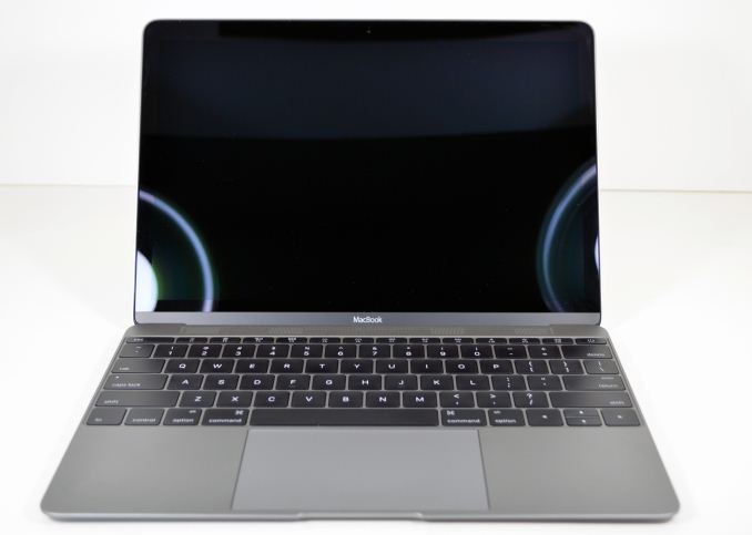
The ever-excellent crew over at iFixit completed their initial teardown of the Early 2015 MacBook yesterday, creating some very nice shots of the Mac’s little logic board in the process. However not stopping there the crew also detached the SSD controller from the board, giving us our best look yet at what we strongly believe to be an Apple-built semi-custom or fully-custom SSD controller.

On the logic board itself, we can see that iFixit’s sample is equipped with Toshiba MLC NAND, 128GB per side, one package per side. However of greater interest is the chip bordered in orange, which based on the fact that it has multiple markings we believe to be the SSD controller, assembled in a Package-On-Package (PoP) fashion. The number we can decode is a part number for a 512MB Hynix LPDDR3 memory module; the other number we cannot decode at this time.
Multiple markings in this fashion is a tell-tale sign of a PoP chip, and having the SSD controller and its DRAM on-package with each other and located right next to the NAND chips makes a ton of sense, especially in such a cramped design. That said, while it means we can’t directly access the SSD die, it also confirms that this is not a strictly off-the-shelf SSD controller since someone had to go through the extra step of PoPing it.
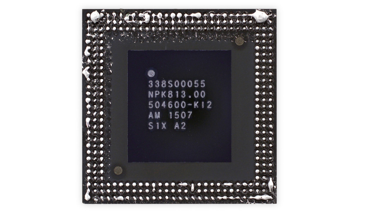
Meanwhile having detected the chip from the logic board, we can see the underside of the chip, which has additional markings. At this time we are unable to decode the part number, 338S00055, though based on the location and PoP design we believe it to be the SSD controller. Otherwise the fact that it doesn’t match any other SSD controller part numbers is yet another clue that Apple had some kind of hand in developing the SSD controller.
Apple in traditional fashion is mum on the whole matter, but we’ll keep digging to see what else we can uncover about this unexpected surprise in their latest laptop.
Source: iFixit


34 Comments
View All Comments
JJ Wu - Monday, April 27, 2015 - link
Apple uses 4Gb LPDDR2 to the RAM SSD controller needs. As iFixit found, there is one SK Hynix LPDDR2(it is not LPDDR3 as iFixit said.). Apple uses PoP package to put the LPDDR2 above the SSD controller and the package is Apple customized PoP.jay5 - Friday, April 17, 2015 - link
I think the elpida RAM is used by the Broadcom "network processor" (the chip highlighted in light blue). If you look at motherboards from the other Macbook lines you will see a similar configuration.Samus - Friday, April 17, 2015 - link
The size could also be from a large SRAM.repoman27 - Thursday, April 16, 2015 - link
Your sense of scale may be a bit off due to how tiny that PCB is (~37mm x 110mm). The SSD controller is right around 15.5 mm x 15.5 mm. It's almost a mm smaller per side than Samsung's UBX controller for the SM951. I highly doubt it's an FPGA. Just for the sake of power efficiency alone, Apple wouldn't go that route.Pissedoffyouth - Friday, April 17, 2015 - link
Encryption engine? VRAM?willis936 - Friday, April 17, 2015 - link
Then spin an ASIC. FPGA is the last chip you'd want to put in a thin, low power device.Einy0 - Saturday, April 18, 2015 - link
Good point, both of them... Apple is adept at designing new silicon and getting it ready without an leaks. My only question is, if they designed this and it is even a decent performer, why didn't they toot their own horn about it when they announced the Macbook? They do about everything else they design.solipsism - Sunday, April 19, 2015 - link
I seem to recall they did mention the SSD being 2x faster.repoman27 - Thursday, April 16, 2015 - link
What confuses me is the other discrete DRAM package. You've got the 512 MB SK Hynix LPDDR2-1066 stacked with the SSD controller, but then what's that other 512 MB of Elpida DDR3L-RS 1600 doing there?repoman27 - Thursday, April 16, 2015 - link
(ninja'd by extide on my last comment)But once again, to put the size of that PCB in perspective, it's not much larger than an m.2 2280 SSD which is only 22 mm x 80 mm.