Estimating Intel-Micron 32-layer 3D NAND Die Size
by Kristian Vättö on March 27, 2015 5:55 AM EST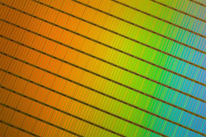
Yesterday Intel and Micron shared some new details of their 3D NAND technology and during the presentation they also showed a production wafer. I missed the wafer during the live broadcast (hence I couldn't include this in the initial write up), but fortunately Intel-Micron have now posted the recorded webinar, which I used to get a pretty good shot of the wafer. The quality isn't perfect, but it's good enough that I was able to make a fairly accurate estimation of the die size.
Disclaimer: The data and analysis presented in this article is based on estimations that are provided "as is" with no guarantee of full accuracy.
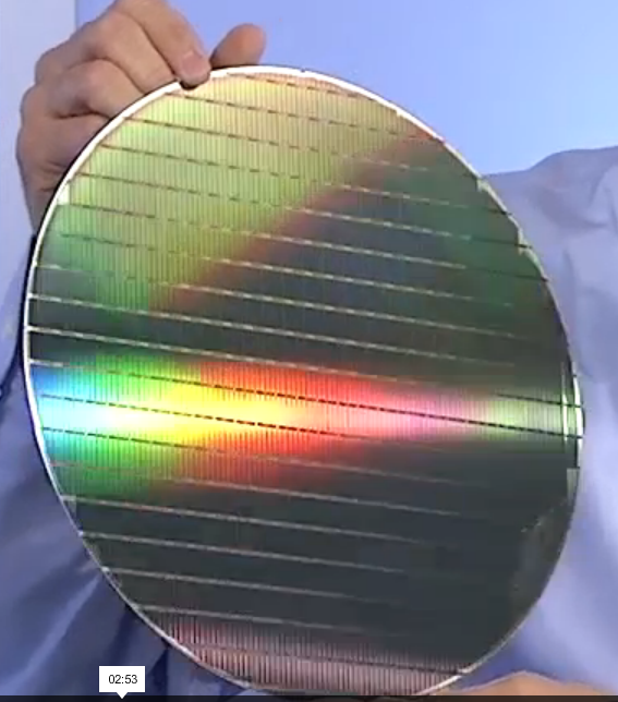
I calculated 19 dies vertically and 25 horizontally, which would yield a die size of 189.5mm. That's a bit too high since it doesn't take the partial dies on the edges of the wafer into account, so when taking that and the die cuttings (i.e. the space between dies) into account, my estimation of the die size would be 175mm. I think in reality it might be closer to 170mm, but I'll rather be conservative than present too optimistic numbers.
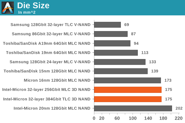
My die size estimation goes pretty well hand-in-hand with Intel-Micron's planar NAND dies. The two have never really focused on building small dies for mobile applications (e.g. microSD cards), which is why the die sizes are higher compared to the others with mobile focus. I was told Intel-Micron might build a smaller two-plane 3D NAND for mobile use if they see demand for it, but as I mentioned in yesterday's news post the initial die will be a 4-plane design that is aimed for SSDs.
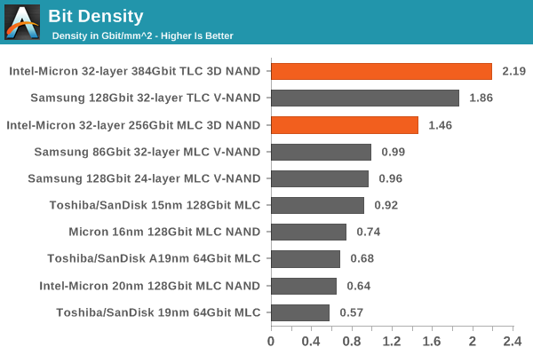
Now that we have the die size we can also estimate the most important metric i.e. the bit density. Intel-Micron's 32-layer 3D NAND design is by far more efficient than Samsung's, which is mostly explained by the much higher die capacity. The memory array efficiency (i.e. the portion of the die that's dedicated to memory cells) tends to scale with die capacity because the peripheral circuitry doesn't need too many modifications and thus the die area taken by the circuitry doesn't really increase with capacity.
I estimated Intel-Micron's 32-layer 3D NAND to have array efficiency of approximately 85%, which is very good and considerably higher than Samsung's 32-layer design (66% for the 86Gbit MLC part and 72% for the 128Gbit TLC part). Samsung did some peripheral circuitry optimizations for the 32-layer TLC part that explain the higher array efficiency versus the MLC part. When assuming similar array efficiencies for Intel-Micron and Samsung TLC dies, the bit densities are actually equivalent, suggesting that from a lithography and cell size perspective the two designs should be quite similar.
I now understand why Intel-Micron claim that their 3D NAND technology comes with disruptive cost because it really is the most efficient 3D NAND technology we have seen so far. It has twice the bit density compared to Micron's latest 16nm 128Gbit die, which should be enough to mitigate the higher production cost per wafer and make 3D NAND a natural successor to Intel-Micron's planar NAND. It will be interesting to see how Samsung's third generation V-NAND stacks up against Intel-Micron's 32-layer 3D NAND, but it's clear that Samsung must be able to increase the die capacity to remain competitive as it's more than just a game of layers.


36 Comments
View All Comments
jjj - Friday, March 27, 2015 - link
Maybe you could try to ask one of the NAND makers to give you some indication of how the costs change with the number of layers. They won't provide precise numbers but some wide range would be ok.And ofc we all ignore packaging costs , those are a significant factor when it comes to cheap chips (and NAND is relatively cheap).
extide - Friday, March 27, 2015 - link
Die size is still very important, because it determines how many die can fit on a wafer, and thus directly influences the cost.ats - Friday, March 27, 2015 - link
It has some effect but less than most think when you get into dies with lots and lots of layers. When you get into 32 to 48 layer dies, you costs are going to be overwhelmingly dominated by processing costs. A 48 layer die is looking at well over 100 Litho steps. The cost savings of the multi-layer dies come from the planar dies requiring multiple patterning litho steps. Most of the equipment is going to be the same between a multi-layer nand and planar nand (even at 19-15nm). Where you'll save is likely faster throughput per litho step (older easier to work with resist, less precise etch requirements, etc). If the throughput per wafer is overall higher with multi-layer, then the cost per area for multi-layer will be cheaper, if it isn't, then it won't.jjj - Friday, March 27, 2015 - link
All i said was that it matters less not that it doesn't matter at all.Anyway , bare die is cheap, what matters is what you do with it. Here is a quote from a report that's some 6 months old ,sadly i don't remember the source. (they are talking revenue per wafer for the foundry)
"There is more than a 14 times difference between 0.5-micron 200mm revenue per wafers (US$430) and 28nm 300mm revenue per wafers (US$5,850). Even when normalizing the figures by using revenue per square inch, the difference is dramatic (US$51.77 for the 28nm technology versus US$8.56 for the 0.5-micron technology)."
To make it easier for some ,a square inch is 645.16 square mm.
Ofc there are yields and other costs not just the wafer.
So here you got different numbers of layers (impacting cost and yield), Intel using floating gate vs others charge trap, maybe different processes so the costs per square inch can be very different.
Kristian Vättö - Saturday, March 28, 2015 - link
3D NAND requires a whole new set of deposition and etch tools because the tools used for planar NAND aren't designed for depositing dozens of layers and the etch tools aren't capable of such high aspect ratio etching with the precision required. 3D NAND basically moves the difficulty away from lithography/patterning to deposition and etching.ats - Saturday, March 28, 2015 - link
I'm not so sure about new depo and etch tools. The process of CVD is pretty much independent of layer count and etch is also pretty much independent of layer count. They may be using newer tools with increased deposition rates but those new tools would work just as well with planar. And etching is that heavily tool based, its primarily chemistry.Now it may require new deposition, etch, and polishing techniques/formulas, but the equipment should be the same. The mechanics though of those three things really don't change at all.
Etch is still dip wafer in aggressor agent for set time period. CVD is still put wafer in vacuum chamber for set amount of time, etc.
They way to get to things like high aspect ratios is via recipe manipulations and barrier manipulations.
JatkarP - Friday, March 27, 2015 - link
I heard this is the first use of a floating gate cell in 3D NAND. What did samsung use then for 850 EVO ?Kristian Vättö - Friday, March 27, 2015 - link
Samsung's V-NAND uses a charge trap instead of a floating gate.jhgf1000 - Friday, March 27, 2015 - link
How does the number of layers affect the cost? Intel's has 32 layer while the others will have 48.Kristian Vättö - Friday, March 27, 2015 - link
The production cost per wafer is higher since there are more steps to build a 48-layer die, but the increased bit density overrules that, which makes a 48-layer chip generally more cost effective than 32-layer (assuming similar yields, array efficiency etc.).Note that Toshiba-SanDisk won't enter mass production until H1'16, so Intel-Micron has an advantage in terms of entering the market and will likely have 2nd gen in mass production before Toshiba-SanDisk. Samsung's 3rd gen V-NAND is still a question mark.