The NVIDIA GeForce GTX 980 Review: Maxwell Mark 2
by Ryan Smith on September 18, 2014 10:30 PM ESTMaxwell 1 Architecture: The Story So Far
Before we dive into the story and architecture of Maxwell 2, we’d like to spend a bit of time recapping what we’ve seen so far with Maxwell 1 and the GM107 GPU. While both GPUs are distinctly Maxwell, Maxwell 2 is essentially a second, more feature-packed version of Maxwell. Meanwhile it retains all of the base optimizations that went into Maxwell 1, implemented on a larger scale for a larger GPU.
Beginning with the Maxwell family of architectures, NVIDIA embarked on a “mobile first” design strategy for GPUs, marking a significant change in NVIDIA’s product design philosophy. As of Maxwell NVIDIA’s top-down philosophy that saw the launch of high-end desktop class GPUs come first has come to an end, and as NVIDIA has chosen to embrace power efficiency and mobile-friendly designs as the foundation of their GPU architectures, this has led to them going mobile first on Maxwell. With Maxwell NVIDIA has made the complete transition from top to bottom, and are now designing GPUs bottom-up instead of top-down.
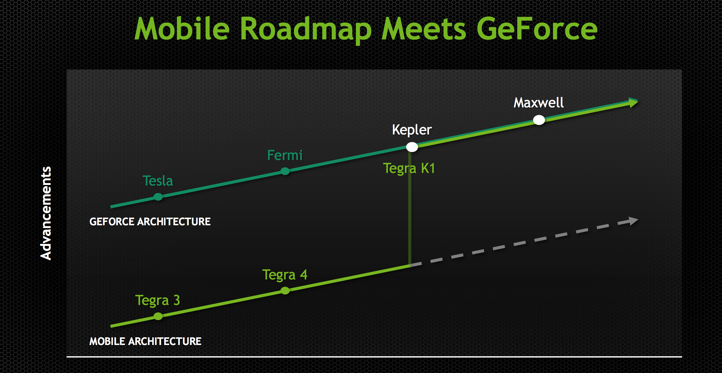
By going mobile first NVIDIA is aiming to address several design considerations at all once. First and foremost is the fact that NVIDIA is heavily staking the future of their company in mobile, and that means they need GPU designs suitable for such a market. This mobile first view is primarily focused on SoC-class products – the Tegra family – but really it even extends to mobile PC form factors such as laptops, where discrete GPUs can play an important role but are going to have strict thermal requirements. By designing GPUs around mobile first, NVIDIA starts with a design that is already suitable for Tegra and then can scale it up as necessary for laptop and desktop GeForce products. Graphics is – as we like to say – embarrassingly parallel, so if you can build one small module then it’s relatively easy to scale up performance by building chips with more modules and tying them together. This is the mobile first philosophy.
What this means is that NVIDIA is focused on power efficiency more than ever before. The SoC market is brutal for both the demands placed on the hardware and for the competitive nature of that market, and given the fact that SoCs are so heavily constrained by thermal and power considerations, every bit of power saved can be reinvested in additional performance. This in turn calls for a GPU that is especially power efficient, as it is efficiency that will win the market for NVIDIA.
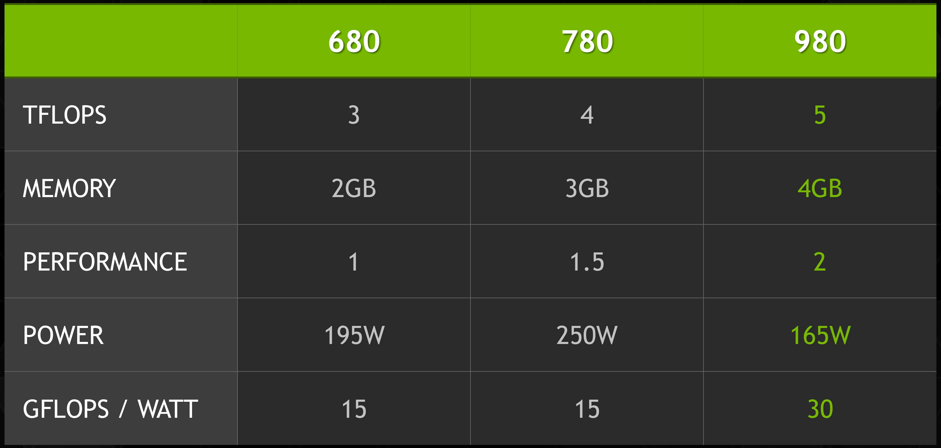
Maxwell then is an interesting take on NVIDIA’s designs that does not radically alter NVIDIA’s architecture, but has had every accommodation made to improve energy efficiency. The result is a Kepler-like architecture with a number of small design tweaks that improve efficiency in some manner. As NVIDIA tells it, there is no single aspect of Maxwell that is disproportionally responsible for NVIDIA’s energy improvements, but rather it is the culmination of these small changes. Through these changes NVIDIA has been able to come close to doubling their performance per watt versus Kepler, which is nothing short of amazing given the fact that all of this is being done on the same 28nm process as Kepler.
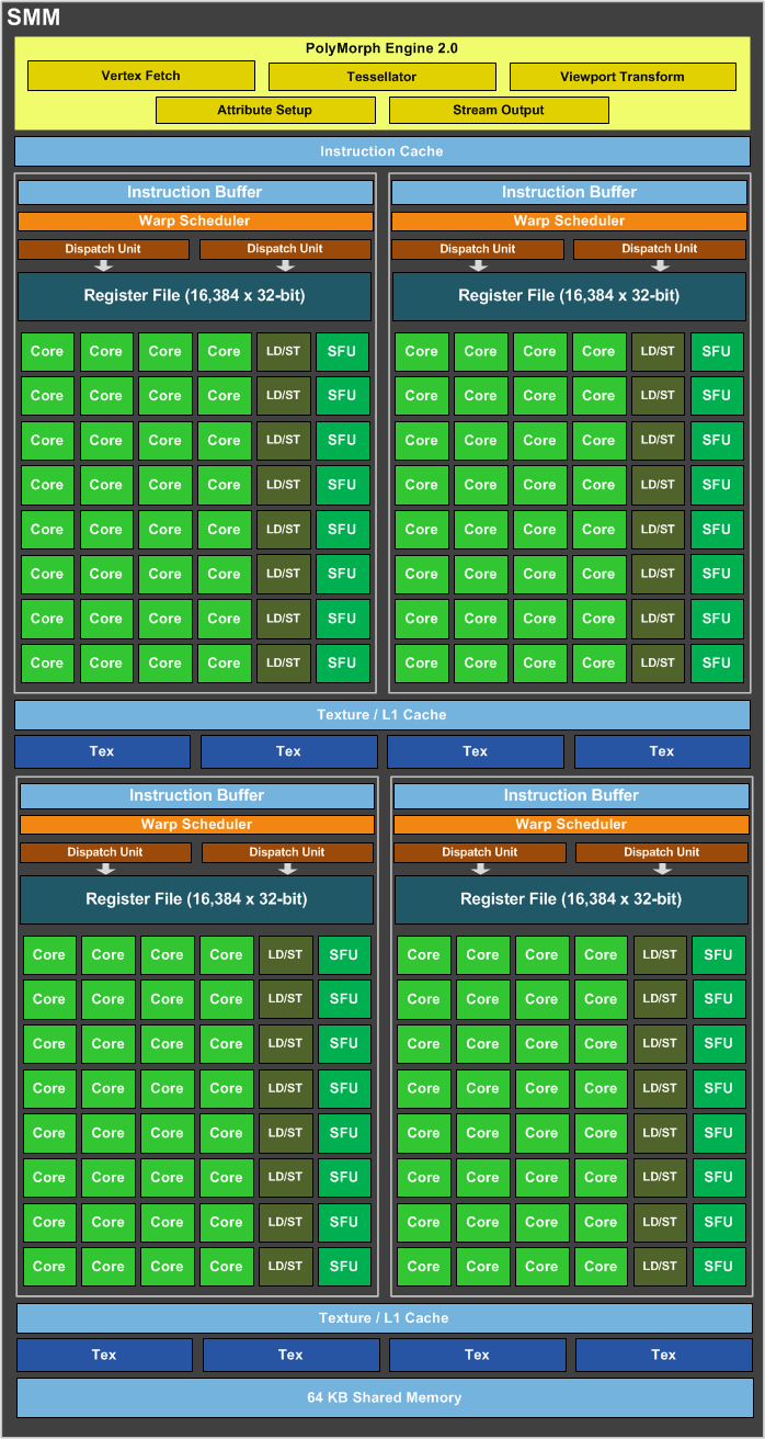
Starting with the Maxwell 1 SMM, NVIDIA has adjusted their streaming multiprocessor layout to achieve better efficiency. Whereas the Kepler SMX was for all practical purposes a large, flat design with 4 warp schedulers and 15 different execution blocks, the SMM has been heavily partitioned. Physically each SMM is still one contiguous unit, not really all that different from an SMX. But logically the execution blocks which each warp scheduler can access have been greatly curtailed.
The end result is that in an SMX the 4 warp schedulers would share most of their execution resources and work out which warp was on which execution resource for any given cycle. But on an SMM, the warp schedulers are removed from each other and given complete dominion over a far smaller collection of execution resources. No longer do warp schedulers have to share FP32 CUDA cores, special function units, or load/store units, as each of those is replicated across each partition. Only texture units and FP64 CUDA cores are shared.
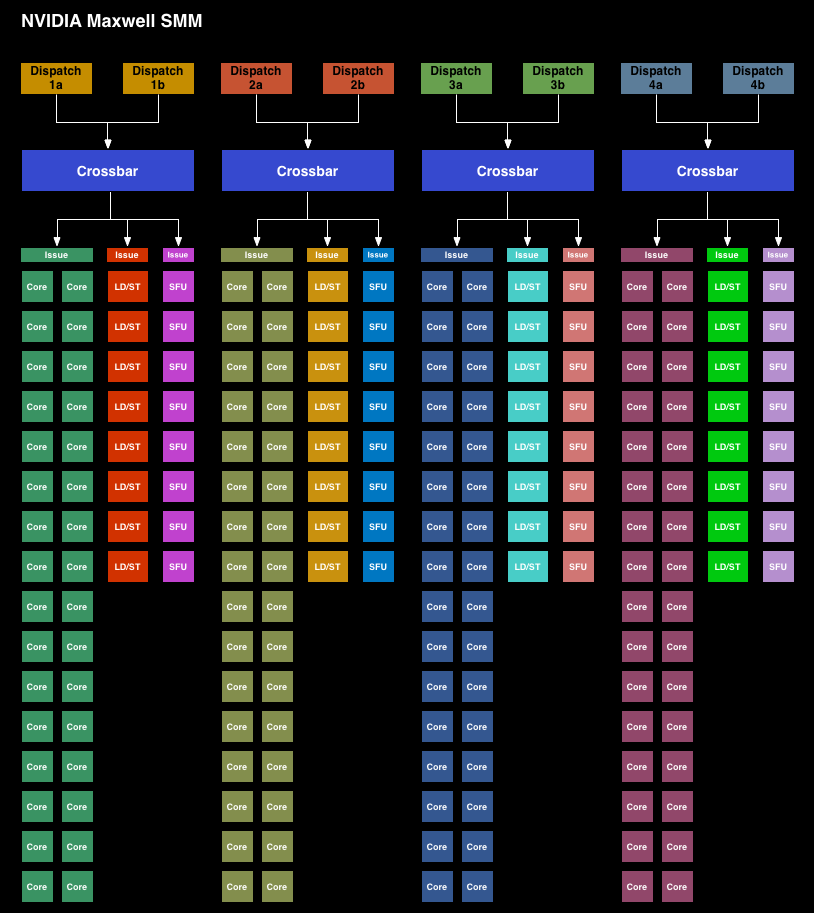
Among the changes NVIDIA made to reduce power consumption, this is among the greatest. Shared resources, though extremely useful when you have the workloads to fill them, do have drawbacks. They’re wasting space and power if not fed, the crossbar to connect all of them is not particularly cheap on a power or area basis, and there is additional scheduling overhead from having to coordinate the actions of those warp schedulers. By forgoing the shared resources NVIDIA loses out on some of the performance benefits from the design, but what they gain in power and space efficiency more than makes up for it.
NVIDIA still isn’t sharing hard numbers on SMM power efficiency, but for space efficiency a single 128 CUDA core SMM can deliver 90% of the performance of a 192 CUDA core SMX at a much smaller size.
Moving on, along with the SMM layout changes NVIDIA has also made a number of small tweaks to improve the IPC of the GPU. The scheduler has been rewritten to avoid stalls and otherwise behave more intelligently. Furthermore by achieving higher utilization of their existing hardware, NVIDIA doesn’t need as many functional units to hit their desired performance targets, which in turn saves on space and ultimately power consumption.
NVIDIA has also been focused on memory efficiency, both for performance and power reasons, resulting in the L2 cache size been greatly increased. NVIDIA has from 256KB in GK107 to 2MB on GM107, and from 512KB on GK104 to the same 2MB on GM204. This cache size increase reduces the amount of traffic that needs to cross the memory bus, reducing both the power spent on the memory bus and improving overall performance.
Increasing the amount of cache always represents an interesting tradeoff since cache is something of a known quantity and is rather dense, but it’s only useful if there are memory stalls or other memory operations that it can cover. Consequently we often see cache implemented in relation to whether there are any other optimizations available. In some cases it makes more sense to use the transistors to build more functional units, and in other cases it makes sense to build the cache. The use of 2MB of L2 cache in both GM107 and GM204 – despite the big differences in ROP count and memory bus size – indicates that NVIDIA’s settling on 2MB as their new sweet spot for consumer graphics GPUs.
Finally there’s the lowest of low level optimizations, which is transistor level optimizations. These optimizations are something of a secret sauce for NVIDIA, but they tell us they’ve gone through at the transistor level to squeeze out additional energy efficiency as they could find it. Given that TSMC 28nm is now a very mature process with well understood abilities and quirks, NVIDIA should be able to design and build their circuits to a tighter tolerance now than they would have been able to when working on GK107 and GK104 over 2 years ago.


274 Comments
View All Comments
Dribble - Friday, September 19, 2014 - link
Looks at prominently placed "AMD CENTRE" link at top of page.wolfman3k5 - Friday, September 19, 2014 - link
Don't forget, this is a prominent pro Intel/NVIDIA site. What did you expect?!Samus - Friday, September 19, 2014 - link
That's because everything AMD touches is a joke. ATI was at the top of their game, far ahead of NVidia on price:performance, then AMD buys them. Look where ATI's been at since. GCN is a crappy architecture. The Netburst of GPU's. Ridiculously high power consumption. The only corner market is has is FP64. If you actually game, GCN is a dud. The only reason Sony/Microsoft went with AMD GPU's was because it's the best (only) integrated CPU/GPU solution (something NVidia has no IP) other than Intel which is way too expensive for consoles and still not as good.bwat47 - Friday, September 19, 2014 - link
Until maxwell AMD's gpu's were handily outperfoming nvidia when it came to price/performance. GCN isn't a bad architecture, its just outdated compared to nvidia's brand new one. I'm sure AMD has architecture improvements coming down the road too. This happens all the time with nvidia and AMD where one of them leapfrogs the other in architecture, the cycle will continue. Right now nvidia is ahead with maxwell, but acting like AMD is doomed or saying that their architecture is the 'netburst of gpu's is silly.Laststop311 - Sunday, September 21, 2014 - link
AMD is going to have to perform a miracle to get their performance and energy use close to nvidia. AMD may keep up in performance but they are going to do that with a 300+ watt dual 8 pin required + liquid cooling required or triple slot required cause it's going to hog the power to keep up and surpass nvidia. Nvidia's solution is much more elegant and there is little hope for amd to match thatLaststop311 - Sunday, September 21, 2014 - link
This isnt even counting gm210. When big maxwell drops at 20nm I just don't see how amd will be able to match it. Like I said it will take an engineering miracle from amdYojimbo - Friday, September 19, 2014 - link
There's a difference between bias and impression. At what point does what you call "tempering bias" become a source of bias in and of itself, because one cannot give one's impression? For instance, the removal of branding the R290X reference card "loud" (which it is). I encourage Mr. Smith neither to "temper his bias" nor to get involved in the "ongoing battle between Nvidia and AMD GPUs", and instead to report the facts and relay his honest impression of these facts. If he does this well, I think the majority of readers of this site will support him for attempting to give a real representation of the state of the products available, which is what they are presumably looking for.wolfman3k5 - Friday, September 19, 2014 - link
Looks like these GTX 970 and 980 cards are shit when it comes to compute, especially double precision floating point operations. I don't game, so I don't care about FPS. I do more productive things with video cards though.Laststop311 - Friday, September 19, 2014 - link
than maybe you should buy a workstation card and not a gaming card or at the very least a titan if you cant afford the super outrageously priced quadro's and tesla'sNfarce - Sunday, September 21, 2014 - link
Then you simply aren't the target market for these types of cards. Like Lastop311 said...go bend over for a professional level workstation GPU that most people here care nothing about. :-/