Measuring Toshiba's 15nm 128Gbit MLC NAND Die Size
by Kristian Vättö on August 22, 2014 12:42 PM EST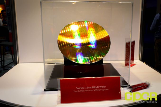
Courtesy of Custom PC Review
At Flash Memory Summit, Toshiba was showcasing their latest 15nm 128Gbit MLC NAND wafer that has been developed in partnership with SanDisk. I simply could not resist to calculate the die size as Toshiba/SanDisk has not published it and die size is always the basis of any semiconductor cost analysis. Unfortunately I was too busy running between meetings that I did not take a photo of the wafer, so I am borrowing the picture from Custom PC Review.
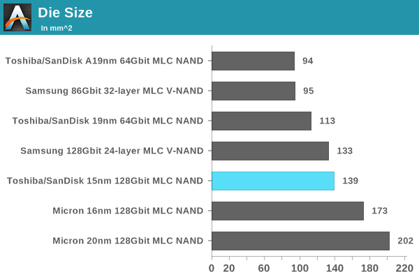
To estimate the die size, I used the same method as with Samsung's second generation V-NAND. Basically I just calculated the amount of dies in both X and Y axes of the wafer as that gives as an approximation of the die size since we know that the diameter of the wafer is 300mm.
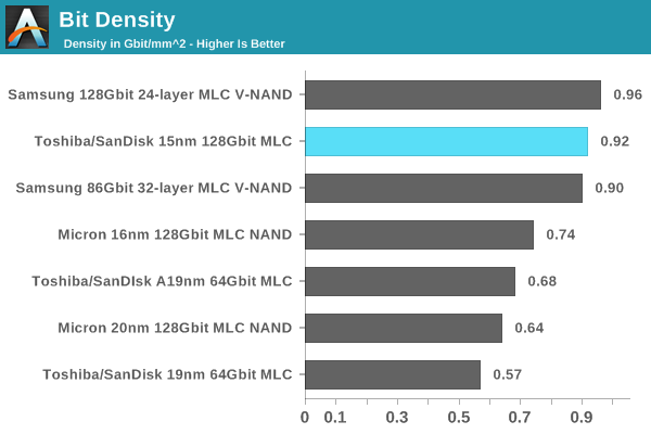
The 15nm node from Toshiba/SanDisk is extremely competitive. Its bit density is essentially equivalent to Samsung's V-NAND, so it is no wonder that Toshiba and SanDisk are betting heavily on their 15nm node before moving to 3D in early 2016. Compared to other 2D NAND dies, the 15nm node is a clear winner from bit density standpoint as Micron's 16nm MLC does not even come close.
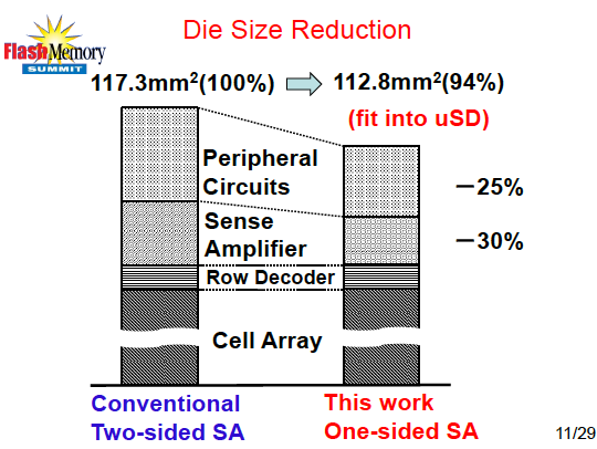
Toshiba's and SanDisk's secret lies in two-sided sense amp and all bit line (ABL) architecture, which reduce the size of the peripheral circuits and sense amplifier, resulting in higher memory array efficiency. Based on my estimation, the array efficiency (i.e. how big portion of the die is dedicated to memory cells) is about 80%, which is typical for a 128Gbit capacity. Higher capacities tend to yield better array efficiency since the peripheral circuitry does not scale as well as the memory cells do, so increasing the die capacity is one of the key solutions in lowering the cost per gigabyte.
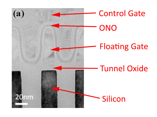
Since nobody has yet taken a cross-section of the 15nm die, it is hard to say for sure what Toshiba and SanDisk are doing to shrink the dimensions. There is no mention of high-K dielectrics, so that seems unlikely and if history is any guidance, then Toshiba/SanDisk is simply increasing the aspect ratio by making the floating gate taller to compensate for the smaller feature size and keep the overall floating gate volume similar. That also helps to maintain the gate coupling ratio because the control gate is still wrapped around the floating gate and with a taller floating gate the capacitance between the gates should remain sufficient despite the increasing proximity of the floating gates.
The production of Toshiba/SanDisk 15nm NAND node is currently ramping up and SSDs based on the new node are expected in Q4'14.


12 Comments
View All Comments
jjj - Saturday, August 23, 2014 - link
Well, they could go with bigger than 64Gb but smaller than 128Gb MLC or some TLC that is small enough but i'm pretty sure nobody is considering 4 bit on such an advanced process , maybe they could on 3D if they use an old process but we don't have details on what process they'll use for 3D and i got the feeling it won't be that old.Hans de Vries - Saturday, August 23, 2014 - link
In September we'll see the 128Gbit 3-bit version of Samsung's 32-Layer, 3-D NAND. This is the same die as the 95mm2 86Gbit 32-Layer die which stores 2-bit per cell. The density increases to 1.35 Gbit/mm2. http://www.businesskorea.co.kr/article/5785/3bit-v...