SanDisk-Toshiba Take Back The Crown With A Different Kind of NAND
by Jason Inofuentes on May 5, 2011 12:01 PM ESTAfter 11 years of partnership, Sandisk and Toshiba's timing could not have been better. Just seven days after losing the NAND crown to Intel and Micron (IMFT) they announce they will have 19nm NAND samples rolling off their fabs as we speak. This one upmanship is normal for this industry but the announcement coming so soon after IMFT's 20nm announcement was a surprise to many. Like IMFT, they expect to start mass production during the second half of this year, and finding homes for their latest NAND in the next wave of tablets, smartphones and SSDs.
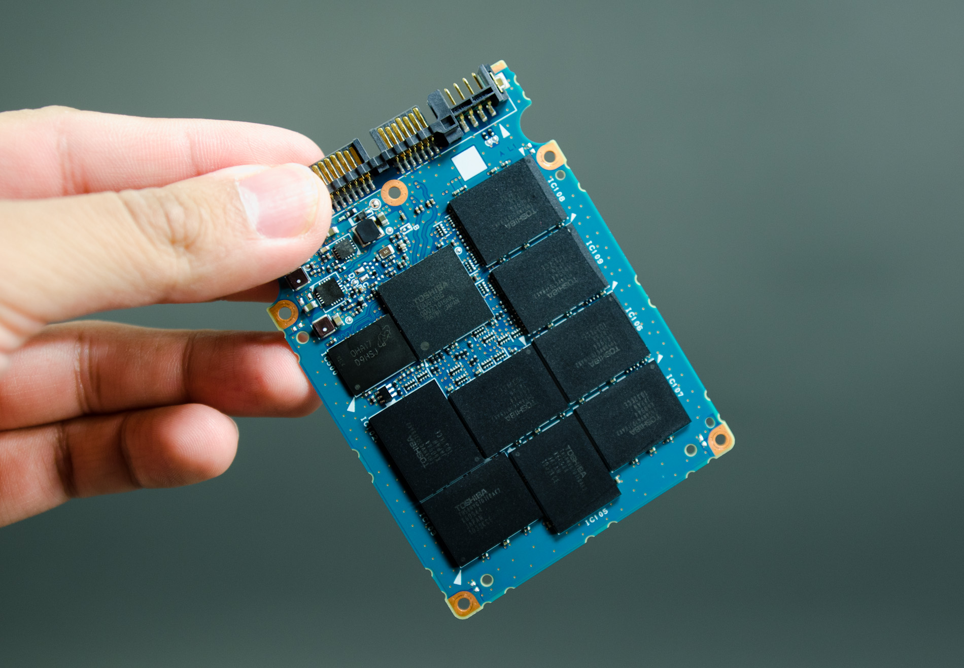
Toshiba NAND on display on the Kingston SSDNow V+100
Anand and I had the opportunity to speak with representatives from Toshiba and SanDisk who sounded quite optimistic about the competitiveness of their 19nm products. Like IMFT, they expect to see similar endurance as their 24nm products, around 3,000 program/erase cycles. This is owing to ever improving ECC and wear leveling algorithms, ensuring as few wasted p/e cycles as possible. SanDisk and Toshiba did not publish die size for this iteration, but did state a decrease of approximately 25%. Previously, their 24nm die size was published as 151mm2, so this iteration should bring that down to about 113mm2, besting IMFT's 118mm2 at 20nm. Page and block sizes remain at their 24nm levels of 8 KB per page and 256 pages per block.
While the benefits for SSDs are the main focus of our NAND coverage, consumer electronics are where the vast majority of readers interact with NAND products. Flash memory is a key component of smartphones, tablets, media players and set-top boxes, in addition to the USB drives and memory cards. Different calibers of NAND are used in these products, with the fastest (SLC) going into enterprise-class SSDs, the mainstream NAND (2-bit MLC) going into your consumer and enthusiast SSDs, phones and tablets and slower products (3-bit TLC and 4-bit 16LC) going into products like jump drives and SD cards. Drawing from Anand's SSD Anthology we recall that the functional difference between SLC and MLC is the amount of data per NAND cell, 1-bit or 2-bits. Adding that extra bit to SLC to make MLC decreases speed and reliability; the same holds true in producing 3-bit NAND. With controllers and ECC algorithms improving, it is likely that 3-bit NAND will be produced in this venture that will end up in more consumer electronics devices, perhaps not your next SSD, but certainly some tablets and smart phones (note that there are 3-bit SSDs floating around in beta form). The benefit for consumers is larger capacity with little price increase and relatively little impact on performance and reliability since consumer electronics devices rarely tax the limits of NAND speed and are designed to endure less than even a conservative estimate for how long the NAND inside should last.
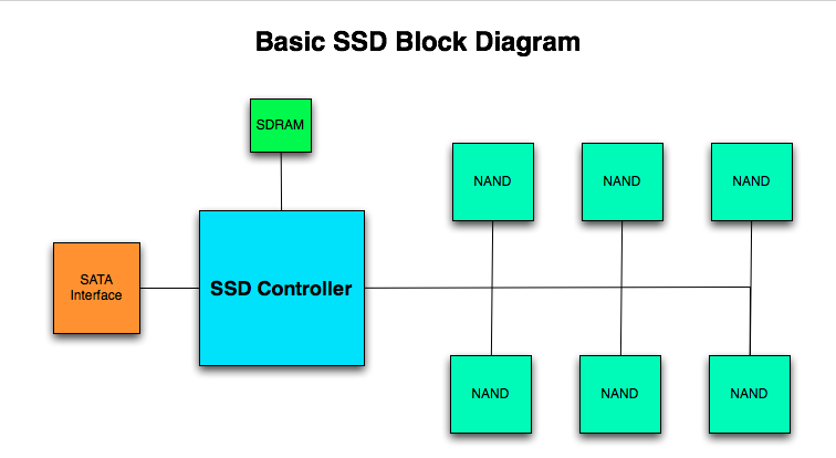
Within the consumer electronics space, however, NAND can be configured in various ways. Above is a block diagram of your average SSD; SATA interface leads to the Controller which uses DRAM to coordinate operations and reads/writes to/from the supply of MLC NAND. Some consumer electronics devices use this exact configuration, as in the Acer Iconia W500 windows tablet. In other devices a similar configuration is used but in an embedded format, where controller and NAND are in a single package soldered to the device's PCB. Still others use raw NAND and utilize the device's own silicon to read/write to the NAND itself, as in all iOS devices. In nearly all of these configurations, volatile memory (DRAM) is used as cache for pending operations (Intel and SandForce excluded, they cache in SRAM); which means that a sudden loss of power could lead to the loss of data that had been waiting to be written to NAND. SanDisk-Toshiba NAND has learned a new trick, apparently present even in the currently shipping 24nm products, that eliminates this risk while also adding a few new options for OEMs.
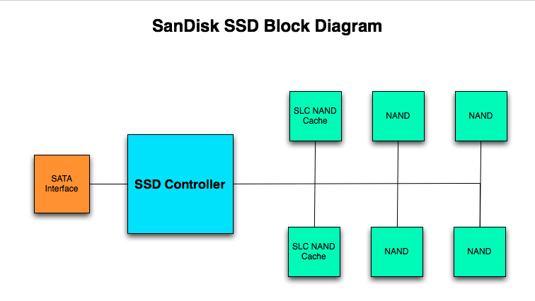
In the block diagram above, gleaned from SanDisk marketing and discussions, DRAM is abandoned in favor of designating a portion of NAND as cache. Data is stored here initially, to be written to MLC during time the controller would otherwise be idle. This area designated as cache isn't just regular MLC NAND, however; it's what was described to us as "pseudo-SLC," treated at the hardware level like SLC but with the narrow voltage deltas of MLC. The benefits are obvious, an increase in speed and reliability, the former of which should mitigate any speed lost from not using SDRAM. Further it seems this pseudo-SLC feature can be used to fill other roles. In its iSSD products, intended for larger consumer electronics devices, SanDisk uses this pseudo-SLC NAND as in the diagram above. A conversation with Toshiba, however, revealed that other OEMs will use psuedo-SLC as speedy reliable storage for firmware (OS) and system files. The technology is manipulated at the block level, and with each block's capacity halved by treating it as SLC, OEMs have a 1MB granularity with which to designate this SLC space for use as cache or as an OS partition.

In their respective press releases, SanDisk and Toshiba both highlight the smartphone and tablet spaces as motivating factors in their drive towards smaller process nodes. Indeed this has been the focus of much of their marketing of late. Their innovations in ECC and this pseudo-SLC technology are tailor made for this space and though no specific devices were named, we are no doubt benefiting from their implementation already.
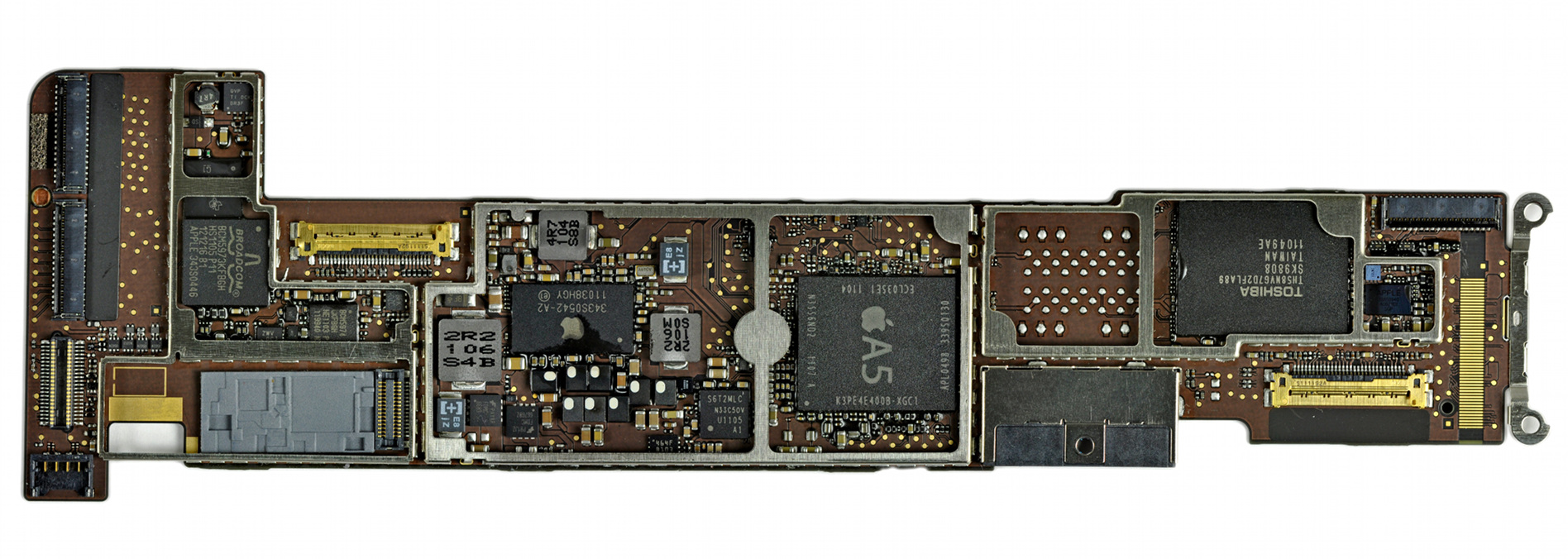
The iPad 2 Mainboard featuring Toshiba NAND, courtesy of iFixit
There are costs to this approach, the main one being . . . well, cost. DRAM is cheap relative to NAND, so sacrificing several blocks of NAND is more expensive than adding 512MB of RAM. Further, though faster than MLC, the writes to SLC NAND are slower than they would be to SDRAM, so a performance penalty is paid. With cost and speed being the driving factors in the consumer SSD space, SanDisk-Toshiba's new trick seems ill suited to the PC space. Enterprise-class SSDs could benefit from the data resilience but these applications are typically laden with power redundancies that provide their SSDs sufficient power to complete any pending writes before losing power. Only in the consumer electronics space is there a strong and growing market for just fast enough, incredibly reliable NAND.


35 Comments
View All Comments
umbrel - Thursday, May 5, 2011 - link
to match DRAM latency?At that point we would not need DRAM at all, just the SSD.
For that matter, how fast a DRAM must be to match L3 cache latency?
cjl - Thursday, May 5, 2011 - link
Much. SSDs have latency of around a hundred microseconds at best right now, while DRAM is under 100 nanoseconds. That's a factor of a thousand or so. L3 cache latency is another factor of 10 or so better than that - around 10 nanoseconds. You won't really reach L3-like latencies with anything that isn't directly on the chip, since at that level, signal travel time becomes fairly significant.JasonInofuentes - Thursday, May 5, 2011 - link
Again, while we don't have confirmation that this is going on, remember that latency can be hidden with speed, or slowness, elsewhere. If the speed between the controller and the pseudo-SLC NAND is faster than the SATA interface (it likely is) then you will not noticethe latency of the pseudo-SLC. There might be a performance penalty in non-cache data that would otherwise reside in SDRAM (think allocation tables).FATCamaro - Thursday, May 5, 2011 - link
Apple has been consistently leapfrogging their competition as opposed to the Apple of old which was always a bit of a follower.Z68 chipset
This new nand
the small ssd's in the MBA
iphone original and on and on.
DigitalFreak - Thursday, May 5, 2011 - link
Point, other than being a fanboi?JasonInofuentes - Thursday, May 5, 2011 - link
Bear in mind that Toshiba doesn't make identifying what features are being used in each implementation, indeed, I haven't been able to figure just what kind of NAND the iPad 2 is using. So while we know that it is Toshiba NAND and while we suspect that it is 24 nm product, so far we only know for certain that Toshiba is implementing this technology in its embedded SmartNAND products.mcnels1 - Thursday, May 5, 2011 - link
On what basis is DRAM cheap relative to NAND? Looking at spot prices, the cheapest DRAM is 97 cents per gigabit ($0.97 for DDR3 1Gb 128Mx8), while the cheapest MLC flash is 22 cents per gigabit ($6.93 for MLC Flash 32Gb 4096Mx8). All prices from memoryexchange.com. Even SLC is cheaper than DRAM ($40.78 for SLC Flash 64Gb 8192Mx8 or 64 cents per gigabit).mindless1 - Thursday, May 5, 2011 - link
It's cheap on the basis of needing less DRAM capacity (512MB for example) to effect a performance increase which is the goal of the larger capacity pseudo-SLC cache in addition to higher reliability.Also remember that this pseudo-SLC is actually MLC chips utilizing only half of each block so your price per Gb listed above needs be doubled for a comparison.
JasonInofuentes - Thursday, May 5, 2011 - link
Also bear in mind that the DRAM used in these devices isn't the DDR3-2200 helping break PCMark records. This is commoditized high volume, low size RAM designed for these specific applications to be as cheap as possible.MrSpadge - Sunday, November 18, 2012 - link
That's why he's looking at the ceapest DRAM, not the most expensive..