The Qualcomm Snapdragon X Architecture Deep Dive: Getting To Know Oryon and Adreno X1
by Ryan Smith on June 13, 2024 9:00 AM ESTOryon CPU Architecture: One Well-Engineered Core For All
For our architectural deep dive, we’ll start with the star of the show: the Oryon CPU core.
As a quick refresher, Oryon is essentially a third-party acquisition by Qualcomm. The CPU core began life as “Phoenix”, and was being developed by the chip startup NUVIA. Comprised of numerous ex-Apple staffers and other industry veterans, NUVIA’s initial plan was to develop a new server CPU core, the likes of which would compete with the cores in modern Xeon, EPYC, and Arm Neoverse V CPUs.
However, seizing the opportunity to acquire a talented CPU development team, Qualcomm purchased NUVIA in 2021. And Phoenix was re-tasked for use in consumer hardware, reborn as the Oryon CPU core.
And while Qualcomm isn’t focusing too much on Oryon’s roots, it’s clear that the first-generation architecture – employing Arm’s v8.7-A ISA – is still deeply rooted in those initial Phoenix designs. Phoenix itself was already intended to be scalable and power efficient, so this is not by any means a bad thing for Qualcomm. But it does mean that there are a number of client-focused core design changes which didn’t make it into the initial Oryon design, and that we should expect to see in future generations of the CPU architecture.
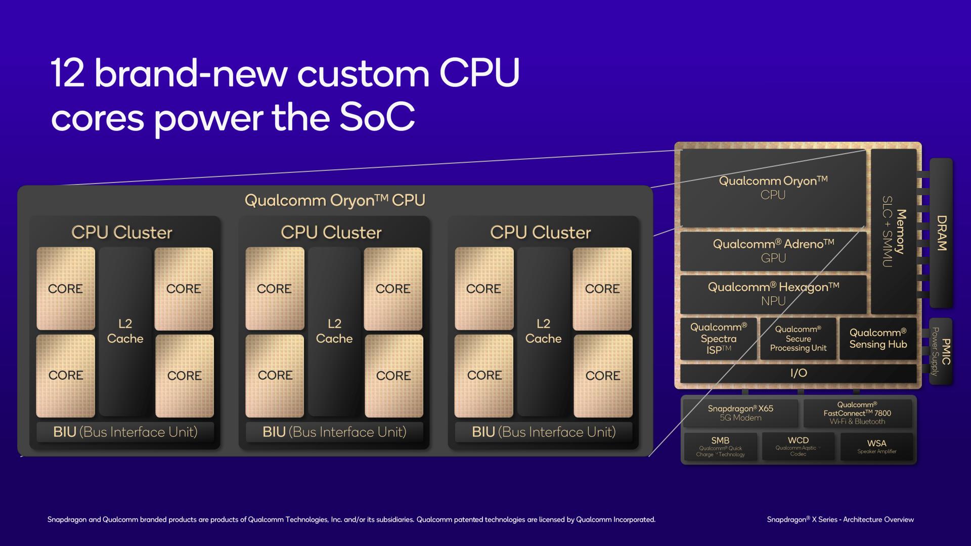
Diving in, as previously disclosed by Qualcomm, the Snapdragon X uses three clusters of Oryon CPU cores. At a high level, Oryon is designed to be a full-scale CPU core, capable of delivering both energy efficiency and performance. And to that end, it’s the only CPU core that Qualcomm needs; there aren’t separate performance-optimized and efficiency-optimized cores like there are on Qualcomm’s previous Snapdragon 8cx chips, or Intel/AMD’s most recent mobile chips, for that matter.
As far as Qualcomm is disclosing, all of the clusters are equal as well. So there isn’t an “efficiency” cluster that’s tuned for power efficiency over clockspeeds, for example. Still, only 2 CPU cores (in different clusters) can hit any given SKU’s top turbo boost speeds; the rest of the cores top out at the chip’s all-core turbo.
Each cluster, in turn, has its own PLL, so each cluster can be individually clocked and powered on. In practice this means that two of the clusters can be put to sleep during light workloads, and then roused from their sleep when more performance is needed.
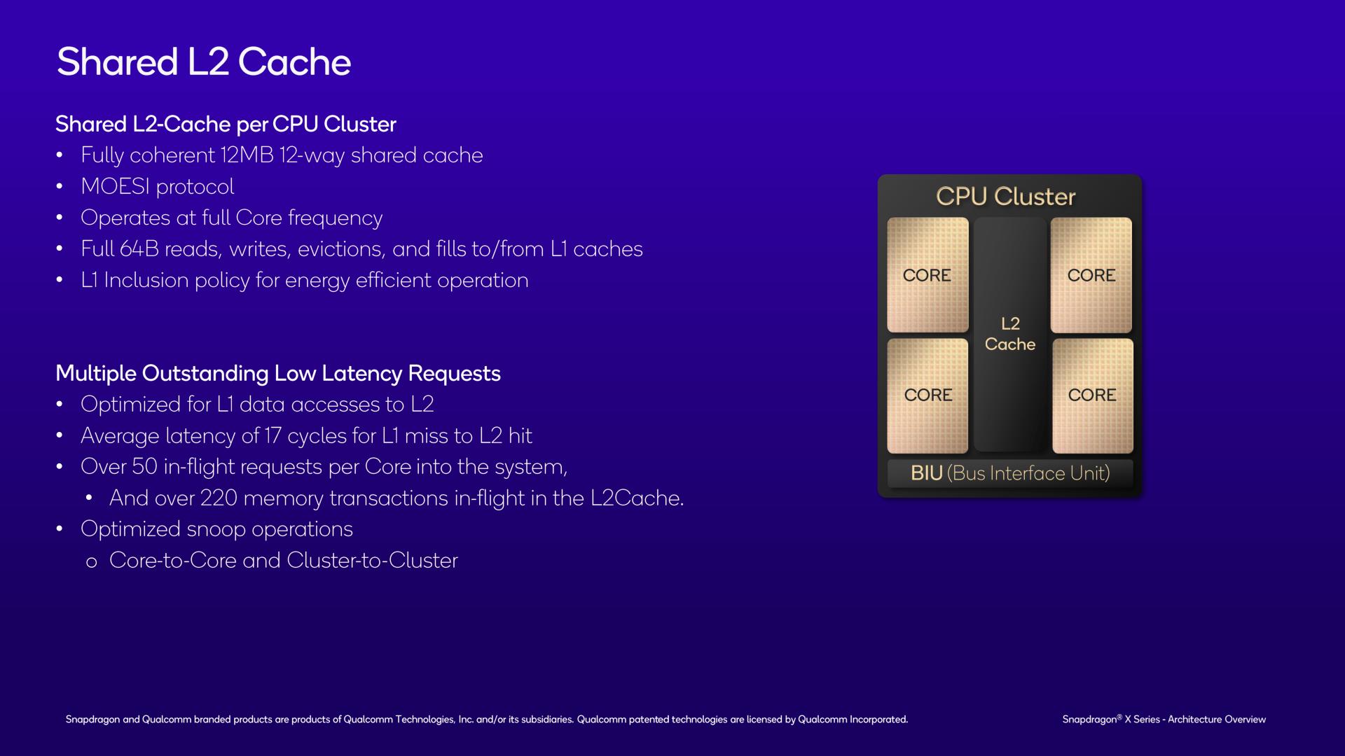
Unlike most CPU designs, Qualcomm is going with a slightly flatter cache hierarchy for Snapdragon X and the Oryon CPU core clusters. Rather than having a per-core L2 cache, the L2 cache is shared per 4 cores (this being very similar to how Intel shares the L2 cache on its E-core clusters). And this is a rather huge L2 cache, as well, at 12MB in size. The L2 cache is 12-way associative, and even with its large size, there’s only a 17 cycle latency to access the L2 cache after an L1 miss.
This is an inclusive cache design, so it contains a mirror of what’s in the L1 cache as well. According to Qualcomm they’re using an inclusive cache for energy efficiency reasons; an inclusive cache means that eviction is much simpler, as L1 data doesn’t need to be moved to L2 to be evicted (or removed from L2 when being promoted to L1). Cache coherency, in turn, is maintained using the MOESI protocol.
The L2 cache itself runs at the full core frequency. L1/L2 cache operations, in turn, are full 64 byte operations, which amounts to hundreds of gigabytes per second of bandwidth between the cache and CPU cores. And while the L2 cache is mostly in place to service its own, directly-attached CPU cores, Qualcomm has implemented optimized cluster-to-cluster snooping operations as well, for when one cluster needs to read out of another.
Interestingly, the Snapdragon X’s 4 core cluster configuration is not even as big as an Oryon CPU cluster can go. According to Qualcomm’s engineers, the cluster design actually has all the accommodations and bandwidth to handle an 8 core configuration, no doubt harking back to its roots as a server processor. In the case of a consumer processor, multiple smaller clusters offers more granularity for power management and as a better fundamental building block for making lower-end chips (e.g. Snapdragon mobile SoCs). But it will come with some trade-offs, with slower core-to-core communication when those cores are in separate clusters (and thus having to go over the bus interface unit to reach another core). It’s a small but notable distinction, since both Intel and AMD’s current designs place 6 to 8 CPU performance cores inside the same cluster/CCX/ring.
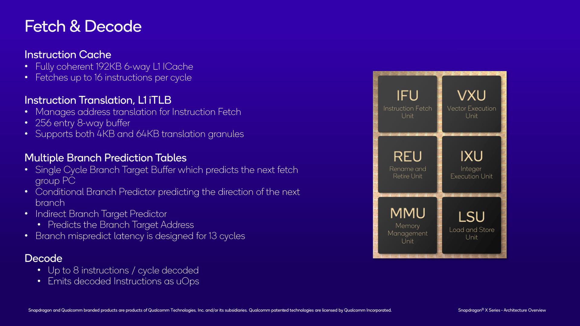
Diving into an individual Oryon CPU core, we quickly see why Qualcomm has gone with a shared L2 cache: the L1 instruction cache in a single core is already massive. Oryon ships with a 192KB L1 I-Cache, three-times the size of the Redwood Cove (Meteor Lake) L1 I-Cache, and even larger still than Zen 4’s. Overall, the 6-way associative cache allows Oryon to keep a lot of instructions very local to the CPU’s execution units. Though unfortunately, we don’t have the L1I latency on-hand to see how it compares to other chips.
Altogether, the fetch/L1 unit of Oryon can retrieve up to 16 instructions per cycle.
That, in turn, feeds a very wide decode front-end. Oryon can decode up to 8 instructions in a single clock cycle, an even wider decode front-end than Redwood Cove (6) and Zen 4 (4). And all of the decoders are identical (symmetrical), so there are no special cases/scenarios required to achieve full throughput.
As with other contemporary processors, these decoded instructions are emitted as micro-ops (uOps), for further processing by the CPU core. Each Arm instruction can technically decode for up to 7 uOps, but according to Qualcomm, Arm v8 in general tends to be much closer to a 1-to-1 ratio of instructions-to-decoded micro-ops.
Branch prediction is another major driver of CPU core performance, and this is another area where Oryon doesn’t skimp. Oryon features all the usual predictors: direct, conditional, and indirect The direct predictor is single-cycle; meanwhile, a branch mispredict carries a 13 cycle latency penalty. Unfortunately, Qualcomm is not disclosing the size of the branch target buffers themselves, so we don’t have a good idea of just how big those are.
We do, however, have the size of the L1 translation lookaside buffer (TLB), which is used for virtual-to-physical memory address mapping. That buffer holds 256 entries, supporting both 4K and 64KB pages.
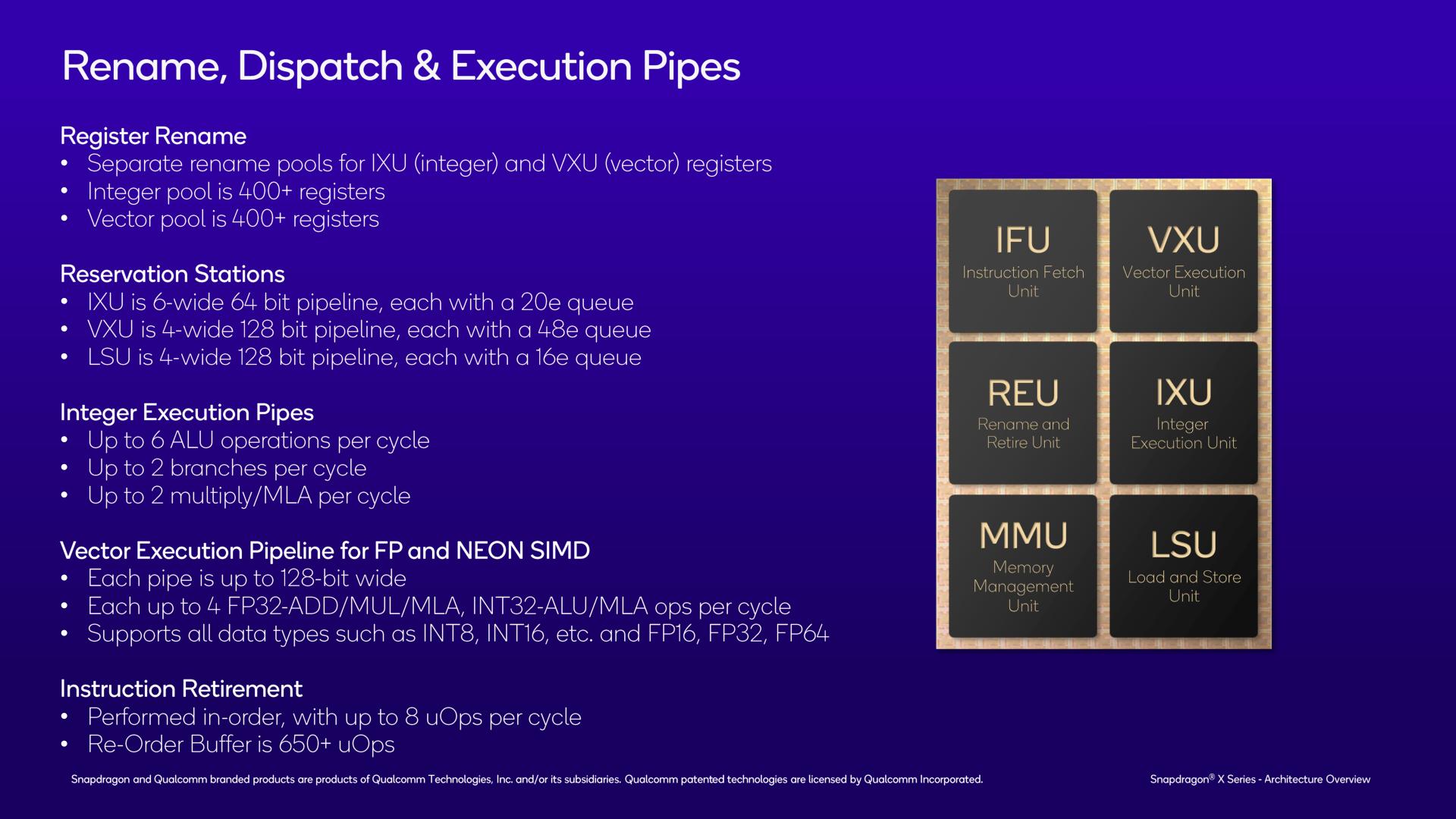
Flipping over to the execution backend of Oryon, there’s a lot to talk about. In part because there’s a lot of hardware and a lot of buffers here. Oryon features a sizeable 650+ re-order buffer (ROB) for extracting instruction parallelism and overall performance through out-of-order execution. This makes Qualcomm the latest CPU designer to throw traditional wisdom out the window and ship a massive ROB, eschewing claims that larger ROBs deliver diminishing returns.
Instruction retirement, in turn, matches the maximum capability of the decoder block: 8 instructions in, 8 uOps out. As noted before, the decoders can technically emit multiple uOps for a single instruction, but most often it’s going to be perfectly aligned with the instruction retirement rate.
The register rename pools on Oryon are also quite massive (are you sensing a common theme here?). Altogether there’s over 400 registers available for integers, and another 400 registers for feeding the vector units.
As for the actual execution pipes themselves, Oryon offers 6 integer pipes, 4 FP/vector pipes, and another 4 load/store pipelines. Qualcomm hasn’t provided a full mapping of each pipeline here, so we can’t run through all the possibilities and special cases. But at a high level, all of the integer pipelines can do basic ALU operations, while 2 can handle branches, and 2 can do complex multiply-accumulate (MLA) instructions. Meanwhile, we’re told that the vast majority of integer operations have a single cycle latency – that is, they execute in a single cycle.
On the floating point/vector side of things, each of the vector pipelines has its own NEON unit. As a reminder, this is an Arm v8.7 architecture, so there aren’t any vector SVE or Matrix SME pipelines here; the CPU core’s only SIMD capabilities are with classic 128-bit NEON instructions. This does limit the CPU to narrower vectors than contemporary PC CPUs (AVX2 is 256-bits wide), but it does make up for the matter somewhat with NEON units on all four FP pipes. And, since we’re now in the era of AI, the FP/vector units support all the common datatypes, right on down to INT8. The only notable omission here is BF16, a common data type for AI workloads; but for serious AI workloads, this is what the NPU is for.
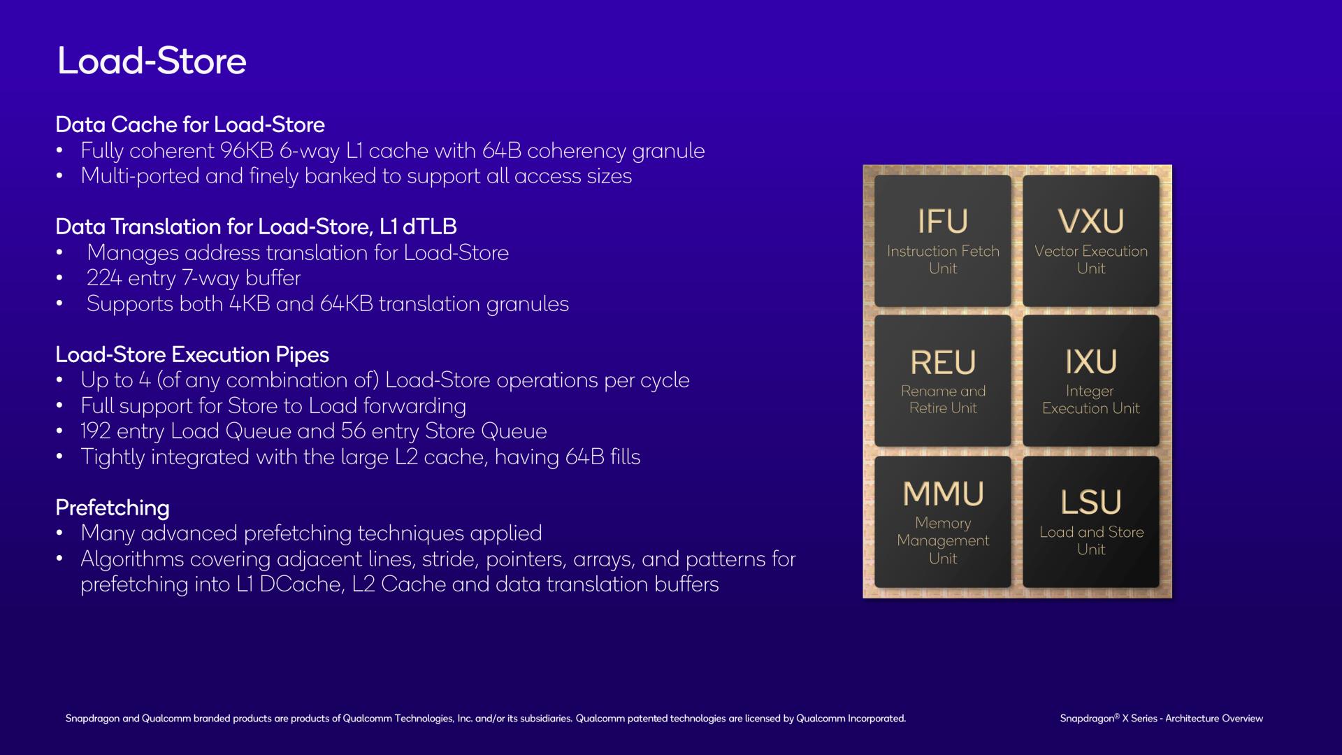
Branching off to its own slide, we have the data load/store units on Oryon. The core’s load/store units are fully flexible, meaning that the 4 execution pipes can do any combination of loads and stores per cycle as needed. The load queues themselves can go up to 192 entries deep, while the store queues can go up to 26 entries. And all fills are the full size of a cache line: 64 bytes.
The L1 data cache supporting the load/store units is also quite sizable in its own right. The fully coherent 6-way associative cache is 96KB in size, twice the size of what you’ll find on Intel’s Redwood Cove (though the upcoming Lion Cove will significantly change this). And it’s finely banked, in order to efficiently support a wide variety of different access sizes.
Otherwise, Qualcomm’s memory prefetcher wanders a bit into “secret sauce” territory, as the company says the relatively complex unit contributes a great deal to performance. Consequently, Qualcomm isn’t saying too much about how their prefetcher works, but it goes without saying that its ability to accurately predict and prefetch data can have a huge impact on the CPU core’s overall performance, especially with how long a trip is to DRAM at modern processor clockspeeds. Overall, Qualcomm’s prefetch algorithms seek to cover multiple cases, ranging from simple adjacencies and strides up to more complex patterns, using past access history to predict future data needs.
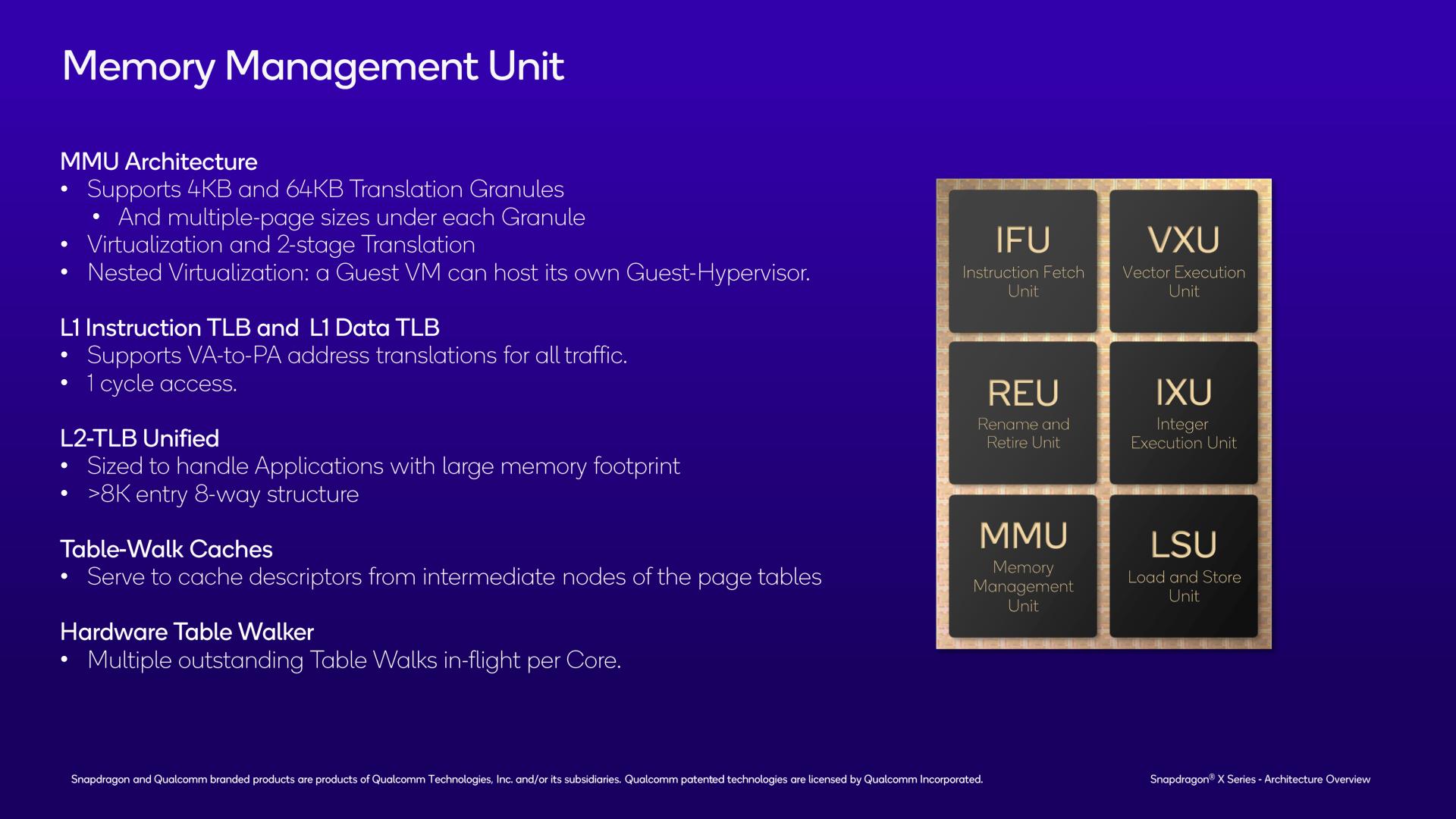
Conversely, Oryon’s memory management unit is relatively straightforward. This is a fully-featured, modern MMU, and it supports even more esoteric features such as nested virtualization – which allows a guest virtual machine to host its own guest hypervisor for even more virtual machines farther down.
Of other notable capabilities here, the hardware table walker is another special mention. The unit, responsible for going out to DRAM if a cache line isn’t in either the L1 or L2 caches, supports up to 16 concurrent table walks. And keep in mind this is per core, so a complete Snapdragon X chip can be doing upwards of 192 table walks at a time.
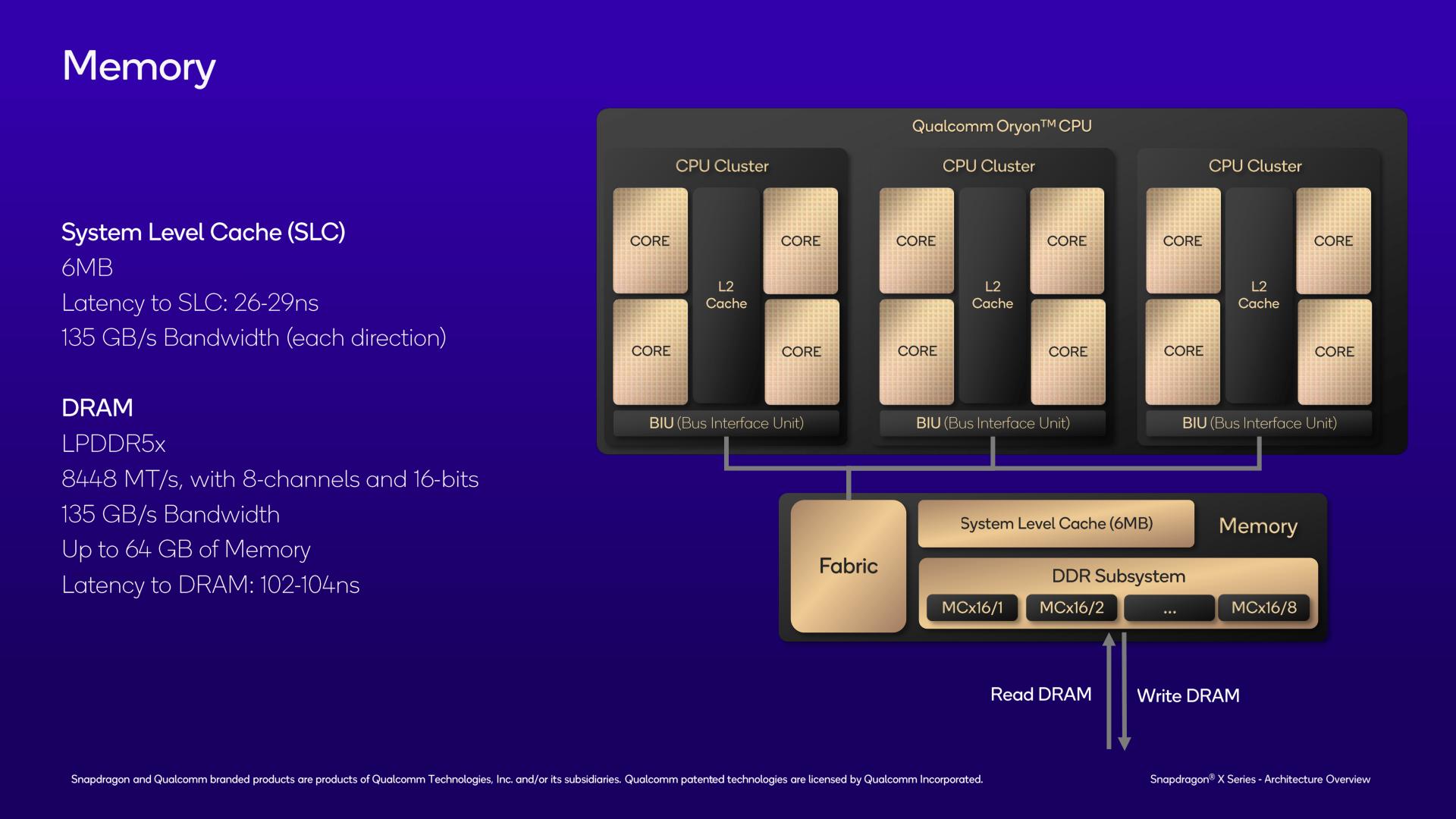
Finally, going beyond the CPU cores and the CPU clusters, we have the highest level of the SoC: the shared memory subsystem.
It’s here where the final level of cache resides, with the chip’s shared L3 cache. Given how big the L1 and L2 caches are for the chip, you might think that the L3 cache would also be quite sizeable. And you’d be wrong. Instead, Qualcomm has outfit the chip with just 6MB of L3 cache, a fraction of the size of the 36MB of L2 cache that it’s backstopping.
With the chip already being cache-heavy at the L1/L2 level, and with the tight integration between those caches, Qualcomm has gone with a relatively small victim cache here to serve as the last stop before going out to system memory. Coming from traditional x86 CPUs, it’s quite a significant change, though it’s very on-brand for Qualcomm, whose Arm mobile SoCs also normally feature relatively small L3 caches. The upside, at least, is that the L3 cache is quite quick to access, at only 26-29 nanoseconds of latency. And it has the same amount of bandwidth as the DRAM (135GB/sec) to pass data between the L2 cache below it and the DRAM above it.
As for memory support, as noted in previous disclosures, Snapdragon X features a 128-bit memory bus with LPDDR5X-8448 support, giving it a maximum memory bandwidth of 135GB/second. At current LPDDR5X capacities, this allows Snapdragon X to address up to 64GB of RAM, though I wouldn’t be too surprised down the line if Qualcomm validates it for 128GB once higher density LPDDR5X chips start shipping.
Notably, unlike some other mobile-focused chips, Snapdragon X does not use on-package memory of any kind. So LPDDR5X chips will go on the device motherboard itself, and it’s up to device vendors to choose their own memory configurations.
With LPDDR5X-8448 memory, Qualcomm tells us that DRAM latency should be just over 100ns, at 102-104ns.
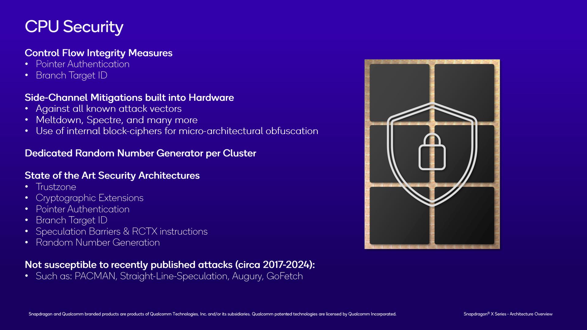
And because this is the last CPU architecture slide, we may as well throw in a quick mention of CPU security. Qualcomm supports all the security features you’d come to expect from a modern chip, including Arm TrustZone, per-cluster random number generators, and security-hardening features such as pointer authentication.
Notably, Qualcomm is claiming that Oryon has mitigations for all known side-channel attacks, including Spectre, an attack that has earned a reputation as “the gift that keeps on giving.” This is an interesting claim as Spectre isn’t really a hardware vulnerability itself, but rather is an inherent consequence of speculative execution. Which in turn is why it’s so difficult to fully defend against (and the best defense is having sensitive operations fence themselves off). None the less, Qualcomm believes that by implementing various obfuscation tools within the hardware, they can protect against these kinds of side-channel attacks. So it will be interesting to see how this plays out.
A Note on x86 Emulation
And finally, I’d like to take a moment to make a quick note on what we’ve been told about x86 emulation on Oryon.
The x86 emulation scenario for Qualcomm is quite a bit more complex than what we’ve become accustomed to on Apple devices, as no single vendor controls both the hardware and the software stacks in the Windows world. So for as much as Qualcomm can talk about their hardware, for example, they have no control over the software side of the equation – and they aren’t about to risk putting their collective foot in their mouth by speaking in Microsoft’s place. Consequently, x86 emulation on Snapdragon X devices is essentially a joint project between the two companies, with Qualcomm providing the hardware, and Microsoft providing the Prism translation layer.
But while x86 emulation is largely a software task – it’s Prism that’s doing a lot of the heavy lifting – there are still certain hardware accommodations that Arm CPU vendors can make to improve x86 performance. And Qualcomm, for its part, has made these. The Oryon CPU cores have hardware assists in place to improve x86 floating point performance. And to address what’s arguably the elephant in the room, Oryon also has hardware accommodations for x86’s unique memory store architecture – something that’s widely considered to be one of Apple’s key advancements in achieving high x86 emulation performance on their own silicon.
Still, no one should be under the impression that Qualcomm’s chips will be able to run x86 code as quickly as native chips. There’s still going to be some translation overhead (just how much depends on the workload), and performance-critical applications will still benefit from being natively compiled to AArch64. But Qualcomm is not fully at the mercy of Microsoft here, and they have made hardware accommodations to improve their x86 emulation performance.
In terms of compatibility, the biggest roadblock here is expected to be AVX2 support. Compared to the NEON units on Oryon, the x86 vector instruction set is both wider (256b versus 128b) and the instructions themselves don’t perfectly overlap. As Qualcomm puts it, AVX to NEON translation is a difficult task. Still, we know it can be done – Apple quietly added AVX2 support to their Game Porting Toolkit 2 this week – so it will be interesting to see what happens here in future generations of Oryon CPU cores. Unlike Apple’s ecosystem, x86 isn’t going away in the Windows ecosystem, so the need to translate AVX2 (and eventually AVX-512 and AVX10!) will never go away either.


51 Comments
View All Comments
FWhitTrampoline - Thursday, June 13, 2024 - link
For the Sake of TechPowerUp's GPU Database That lists the dGPU/iGPUs render configurations as Shader:TMUs:ROPs and (Tensor Cores/Matrix Math Units and RT Units as well) But Please Technology Press adopt some common nomenclature so the Hardware can be as properly quantified as possible. So yes there's different was of stating that but what about the online GPU and CPU information databases and so some standardized taxonomy for CPU and GPU, other processor hardware is needed!And I did Find that slide in your link but please Tech Press for CPU cores and iGPUs/dGPUs please get together on that or maybe see if the ACM has some glossary of terms for CPU Core parts and GPUs as well. As without any standardized nomenclature processors(CPUs, GPUs, NPUs/other) from different makers can not be compared and contrasted to at least some basic level.
I was very Impressed that you referenced and article that's using Imagination Technologies Ray Tracing Hardware Levels classification system as that's a great scholarly way to standardize the classification of the various Hardware Ray Tracing implementations that have appeared since 2014 when the PowerVR Wizard GPU IP appeared with the first hardware based Ray Tracing implementation! Reply
Jonny_H - Thursday, June 13, 2024 - link
The problem with demanding a single consistent comparison number is that hardware isn't consistently comparable between different architectures.Even the RT "levels" you quoted has issues - like AMD GPUs *do* have some hardware acceleration to the BVH processing - just a single node in the tree rather than a hardware tree walker. So it's more than a level 2, but less than a level 3. And there's also the issue that implies they're a linear progression - that level 4 follows level 3, but there's nothing specific about ray coherency sorting that *requires* a hardware BVH tree walker.
Categorizing hardware is complex because hardware implementation details are complex. At some point every abstraction breaks down. Reply
FWhitTrampoline - Thursday, June 13, 2024 - link
Yes things are not directly comparable but TPU's GPU Database does list ROP counts and those "ROPs" usually process 1 Pixel per clock per "ROP" and so the G-Pixel fill rates can be estimated for that and used as a metric to compare different makers GPU hardware for pixel processing numbers(Theoretical Max Numbers).And the RDNA2 GPU micro-architecture received no proper GPU Whitepaper at release and so folks interested in that Ray Tracing on RDNA2 only got some minimal slides sans any in-depth Whitepaper explanation of that, other than a link to the RDNA1 whitepaper that lacked any hardware Ray Tracing at all! And as far as I can tell there was never any formal RDNA2 whitepaper released!
But I do value your Input with regards to the Levels Number for RDNA2's Ray Tracing and is there any reading material out there that you know of that's not behind some NDA that goes into some whitepaper like deep dive into RDNA2's actual RT Pipeline and maybe with some flow charts as well.
The hardest thing for me is Pay-walled Publications and the difficulties around getting access to College Libraries in the large Urban areas of the NE US where that's closed down to students only and no way to get access to that. And so The Microprocessor Report and all the other Trade Journals that I used to have access to when I was in College are not accessible to me now! Reply
GeoffreyA - Friday, June 14, 2024 - link
What about your city's municipal reference library, rather than the lending and university ones? Often, one can get access to different journals there. ReplyFWhitTrampoline - Friday, June 14, 2024 - link
My Public Library is not subscribed to the usual academic Trade and Computing Sciences Journals and lacks the funding. But even with some College Libraries Being federal depository libraries they are not as open to non students as the CFR/USC requires. And so that makes things harder in the NE US. Now if I lived om the West Coast of the US and in some large Urban Area things are different there and even in the Southern US Cities surprisingly. ReplyGeoffreyA - Friday, June 14, 2024 - link
I understand. It's a sad state of affairs for information to be unaccessible. Replymode_13h - Saturday, June 15, 2024 - link
> is there any reading material out there ... that goes into some whitepaper like deep dive> into RDNA2's actual RT Pipeline and maybe with some flow charts as well.
Have you seen this?
https://chipsandcheese.com/2023/03/22/raytracing-o... Reply
name99 - Saturday, June 15, 2024 - link
https://sci-hub.se ReplySoulkeeper - Friday, June 14, 2024 - link
To the few comments complaining about "marketing slides" or no benchmarks ...I appreciate this article, it's a pre release technical overview of a new cpu design.
This kind of technical stuff is what made anandtech great.
We are smart enough to spot the marketing, consume the author's input, and judge for ourselves (and should be patient enough to wait for benchmarks).
Keep up the good work. Reply
AntonErtl - Friday, June 14, 2024 - link
Spectre is not at all an inherent consequence of speculative execution.Speculative execution does not reveal information through architectural state (registers, memory), because CPU designers have been careful to reset the architectural state when detecting a branch misprediction. They have not done this for microarchitectural state, because microarchitecture is not architecturally visible. But microarchitectural state can be revealed through side channels, and that's Spectre.
So the first part of the Spectre fix is to treat microarchitectural state (e.g., loaded cache lines) like architectural state: Buffer it in some place that's abandoned when the speculation turns out to be wrong, or is promoted to longer-term microarchitectural state (e.g., a cache) when the instruction commits (look for papers about "invisible speculation" to see some ideas in that direction). There are also a few other side channels that can reveal information about speculative processed data that need to be closed, but it's all doable without excessive slowdowns.
Intel and AMD have been informed of Spectre 7 years ago. If they had started working on fixes at the time, they would have been done long ago. But apparently Intel and AMD decided that they don't want to invest in that, and instead promote software mitigations, which either have an extreme performance cost, or require extreme development efforts (and there is still the possibility that the developer missed one of the ways in which Spectre can be exploited), so most software does not go there. Apparently they think that their customers don't value Spectre-immunity, and of course they love the myth that Spectre is inherent in speculation, because that means that few customers will ask them why they still have not fixed Spectre.
It's great that the Oryon team attacks the problem. I hope that they produced a proper fix; the term "mitigation" does not sound proper to me, but I'll have to learn more about what they did before I judge it. I hope there will be more information about that forthcoming. Reply