Tenstorrent Licenses RISC-V CPU IP to Build 2nm AI Accelerator for Edge
by Anton Shilov on February 28, 2024 4:30 PM EST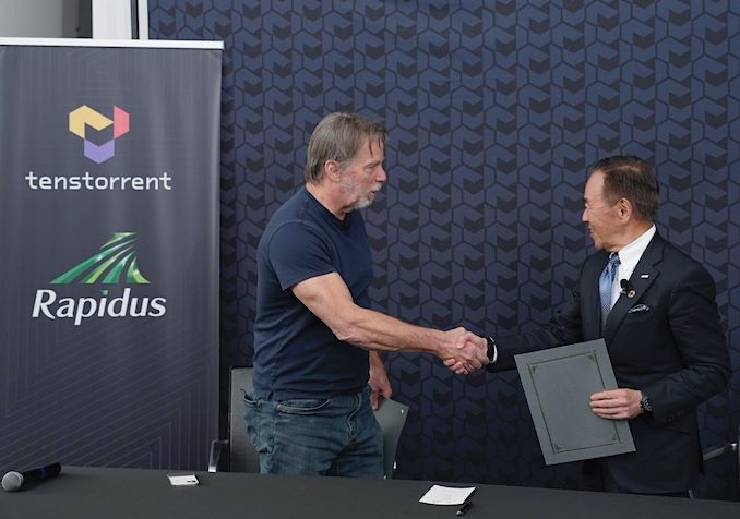
Tenstorrent this week announced that it had signed a deal to license out its RISC-V CPU and AI processor IP to Japan's Leading-edge Semiconductor Technology Center (LSTC), which will use the technology to build its edge-focused AI accelerator. The most curious part of the announcement is that this accelerator will rely on a multi-chiplet design and the chiplets will be made by Japan's Rapidus on its 2nm fabrication process, and then will be packaged by the same company.
Under the terms of the agreement, Tenstorrent will license its datacenter-grade Ascalon general-purpose processor IP to LSTC and will help to implement the chiplet using Rapidus's 2nm fabrication process. Tenstorrent's Ascalon is a high-performance out-of-order RISC-V CPU design that features an eight-wide decoding. The Ascalon core packs six ALUs, two FPUs, and two 256-bit vector units and when combined with a 2nm-class process technology promises to offer quite formidable performance.
The Ascalon was developed by a team led by legendary CPU designer Jim Keller, the current chief executive of Tenstorrent, who used to work on successful projects by AMD, Apple, Intel, and Tesla.
In addition to general-purpose CPU IP licensing, Tenstorrent will co-design 'the chip that will redefine AI performance in Japan.' This apparently means that Tenstorrent does not plan to license LSTC its proprietary Tensix cores tailored for neural network inference and training, but will help to design a proprietary AI accelerator generally for inference workloads.
"The joint effort by Tenstorrent and LSTC to create a chiplet-based edge AI accelerator represents a groundbreaking venture into the first cross-organizational chiplet development in semiconductor industry," said Wei-Han Lien, Chief Architect of Tenstorrent's RISC-V products. "The edge AI accelerator will incorporate LSTC's AI chiplet along with Tenstorrent's RISC-V and peripheral chiplet technology. This pioneering strategy harnesses the collective capabilities of both organizations to use the adaptable and efficient nature of chiplet technology to meet the increasing needs of AI applications at the edge."
Rapidus aims to start production of chips on its 2nm fabrication process that is currently under development sometimes in 2027, at least a year behind TSMC and a couple of years behind Intel. Yet, if it starts high-volume 2nm manufacturing in 2027, it will be a major breakthrough from Japan, which is trying hard to return to the global semiconductor leaders.
Building an edge AI accelerator based on Tenstorrent's IP and Rapidus's 2nm-class production node is a big deal for LSTC, Tenstorrent, and Rapidus as it is a testament for technologies developed by these three companies.
"I am very pleased that this collaboration started as an actual project from the MOC conclusion with Tenstorrent last November," said Atsuyoshi Koike, president and CEO of Rapidus Corporation. "We will cooperate not only in the front-end process but also in the chiplet (back-end process), and work on as a leading example of our business model that realizes everything from design to back-end process in a shorter period of time ever."
Source: Tenstorrent


22 Comments
View All Comments
do_not_arrest - Wednesday, March 6, 2024 - link
The "nm" or "um" rating of a technology was NEVER EVER the transistor pitch. It was ALWAYS the gate length, which is not the same thing. Jeebus read a Wikipedia article. 5/4/3/2 nm technologies typically have gate pitches around the 50nm range. Gate length is now meaningless because the gate construction is so wildly different than the old planar. ReplySantoval - Monday, March 11, 2024 - link
Though it was not clarified I assume "for edge" means AI inferencing, not training right? So this will not compete with Nvidia's GPUs.. Reply