ASML's First High-NA EUV Litho Scanner Arrives At Intel [UPDATED]
by Anton Shilov on January 5, 2024 7:30 AM EST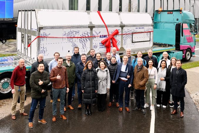
Update 1/5/2024: Intel Oregon announced on Thursday that it has received its shipment of ASML's first-generation Twinscan EXE:5000 High-NA EUV lithography scanner. The two companies will start assembly process of the machine shortly and then Intel will start its High-NA learning curve with the aim to insert the technology into mass production with their post-18A node.
The best way to start the year. 🎊
— Intel News (@intelnews) January 4, 2024
Intel Oregon welcomes major components of @ASMLcompany’s first shipped High-NA EUV technology to help enable the continued and relentless pursuit of Moore’s Law.
Learn more: https://t.co/a5RVr1iWLX pic.twitter.com/NYEUozN4iM
The original story follows as below:
Originally Published: 12/21/2023
ASML on Thursday said that it had shipped its pilot High-NA EUV scanner to Intel. The Twinscan EXE:5000 extreme ultraviolet (EUV) scanner is AMSL's very first High-NA scanner, and it has eagerly been awaited by Intel, who first placed an order for the machine back in 2018. Intel will be using the new machine to experiment with High-NA EUV before it deploys commercial grade Twinscan EXE:5200 tool for high-volume manufacturing (HVM) sometime in 2025. The announcement represents a major industry milestone that will have an impact not only on Intel, but eventually on the other leading-edge fabs as well.
"We are shipping the first High NA system and announced this in a social media post today," a spokesperson for ASML said. "It goes to Intel as planned and announced earlier."
The ASML Twinscan EXE High-NA scanner is set to make its journey from Veldhoven in the Netherlands all the way to Intel's facility near Hillsboro, Oregon, where the tool, jokingly referred to by Intel CEO Pat Gelsinger as Dr. Ann Kelleher's Christmas present, will be installed in the coming months. It is quite a colossal piece of equipment – so large, in fact, that it requires 13 truck-sized containers and 250 crates just to transport it. And once assembled, the machine is 3 stories tall, which has required Intel to build a new (and taller) fab expansion just to house it. It is estimated that each of these High-NA EUV scanners comes with a hefty price tag, likely in the range between $300 million and $400 million.
High numerical aperture (High-NA) EUV lithography tools featuring a 0.55 NA lens are capable of an 8nm resolution, which is a significant improvement compared to current EUV tools with a 13nm resolution. These next-generation High-NA EUV scanners are expected to be important for chip production using process technologies beyond 3nm, which the industry is set to adopt in 2025 – 2026, as they will allow fabs to avoid using EUV double patterning, greatly reducing complexity while potentially enhancing yields and lowering costs.
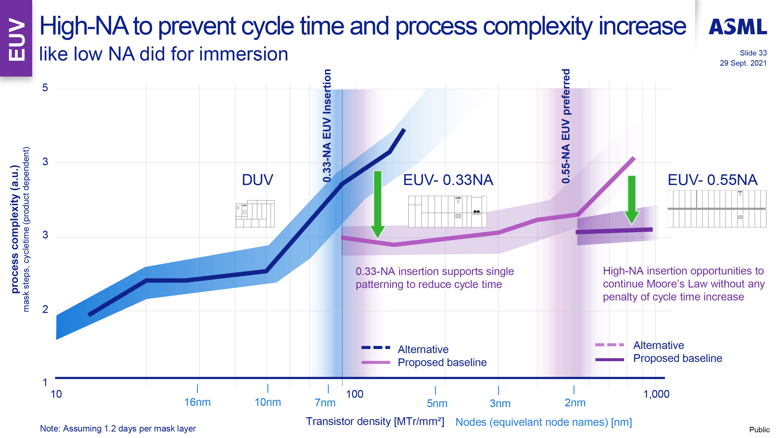
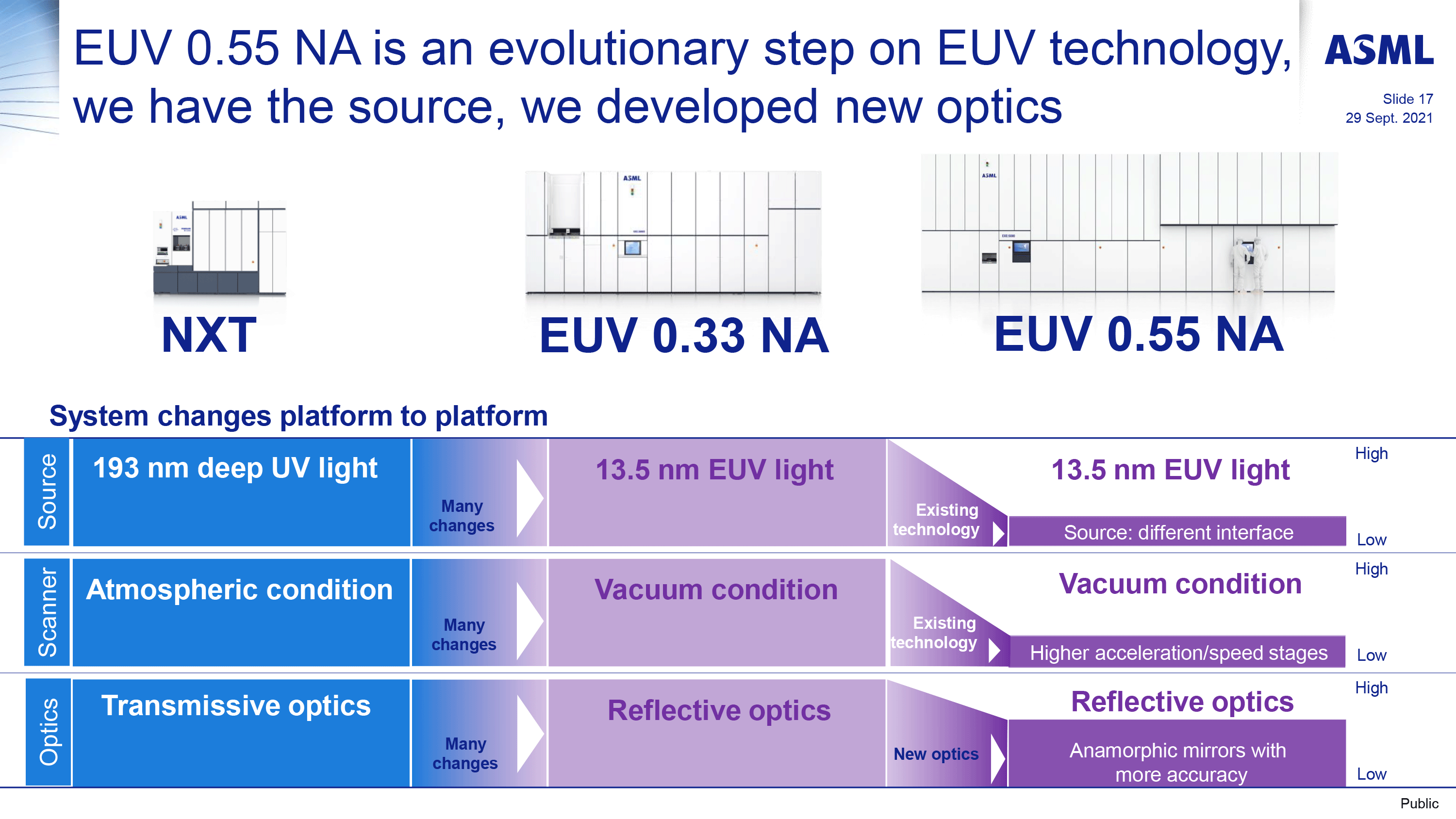
But ASML's Twinscan EXE lithography tools with a 0.55 NA will be significantly different than the company's regular Twinscan NXE litho machines with a 0.33 NA. An avid reader will remember from our previous reports that High-NA scanners are going to be significantly bigger than contemporary EUV scanners, which will require new fab structures. But these is by far not the only difference.
Perhaps the biggest change between the High-NA and regular EUV scanners is the halved reticle size of the High-NA scanners, which will require chipmakers to rethink how they design and produce chips – especially at a time when high-end GPUs and AI accelerators are pushing the limits for reticle sizes. In addition, since High-NA scanners will support a higher resolution and different reticle size, they will require new photoresists, metrology, pellicle materials, masks, and inspection tools, just to name some of the alterations. In short, High-NA tools will require significant investments in infrastructure to go with them.
Although semiconductor production infrastructure is developed by the whole industry, the best way to adopt it for real-world production is to tailor it for actual process technologies and process recipes. Which is why it is so important to start working with pilot scanners early to prepare for HVM using production machines.
Intel was the first company to order ASML's pilot Twinscan EXE:5000 scanner back in 2018. It was also the first to place an order for ASML's commercial grade Twinscan EXE:5200 litho tool in 2022. The company is set to start development work on its 18A node (18 angstroms, 1.8nm) in 2024 and then will employ High-NA tools for a post-18A node, presumably in 2025 – 2026.
By getting High-NA tools earlier than its rivals, Intel not only be able to ensure that its tools produce desired results, but it has a chance to set the standards for the industry when it comes to High-NA manufacturing. For Intel this might mean getting a significant advantage over its rivals, Samsung Foundry and TSMC.
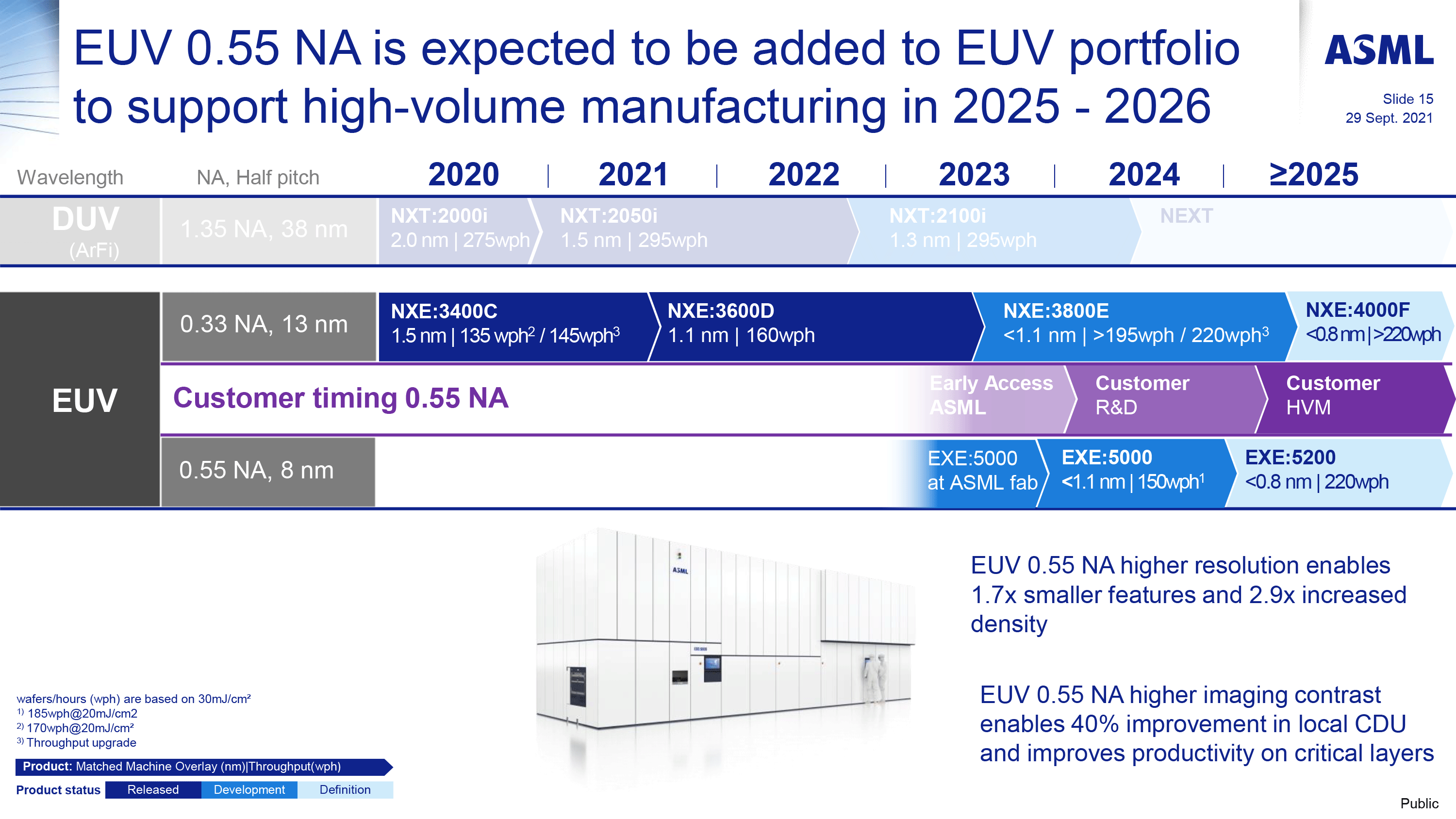
ASML announced in 2022 that it will be able to produce 20 High-NA EUV litho tools per year in 2027 - 2028. Meanwhile, the company disclosed earlier this year is that it had a double-digit number of machines in its High-NA backlog, which signals that its partners are set to adopt these scanners in the coming years. And leading that pack will be Intel.
Source: ASML (X)


28 Comments
View All Comments
Santoval - Friday, December 22, 2023 - link
I truly wonder when this "race to the bottom" will run out of steam and FET transistors of any kind will need to be replaced with a new tech due to physical and/or quantum mechanical limits.GAA-FETs are almost certainly not the last FET tech, TFETs (TunnelFETs) are next. These exploit quantum tunneling, which in traditional MOSFETs is a hindrance, since it increases leakage.
Hence they also overcome the 60 mV/decade of current limit, which is a fundamental limit of MOSFETs. And since they work via quantum tunneling they work best with super slim gates - which, again, does not work well with conventional MOSFETs.
Then what though? Are TFETs the last FET transistors? If so what tech will replace them?
FunBunny2 - Friday, December 22, 2023 - link
"If so what tech will replace them?"in all likelihood, for general deterministic computing, nothing. the so-called quantum computer works only for a miniscule niche of problems. ya ain't gonna run your GL on a computer that guesses at the bottom line.
Threska - Sunday, December 24, 2023 - link
Synaptic Transistors.https://studyfinds.org/synaptic-transistor-human-b...
nandnandnand - Friday, December 22, 2023 - link
If we don't have 10,000-layer CPUs with some kind of integrated cooling, the work isn't done. Stack or slack.Blastdoor - Saturday, December 23, 2023 - link
Graphene?sonicmerlin - Saturday, December 30, 2023 - link
Probably nothing. We reach the limit of what we're capable of with transistors within the universe's laws of physics. We'll have to find a completely new way of computing I guess.evanh - Friday, December 22, 2023 - link
I got a question. Does this High-NA EUV equipment improve on the feature resolution at the same node size? Or, in their promo slides, are they talking about a presumed size node shrink in conjunction?TomWomack - Friday, December 22, 2023 - link
I'm afraid that's rather a confused question; 'node size' and 'feature resolution' are pretty much the same thing, 'node size' is a marketing number referring to a complex specification which includes feature resolution.evanh - Friday, December 22, 2023 - link
The two got divorced a long time back. The marketing term of node size has merrily been partying on fast track, while the more mundane feature resolution stayed home and kept things real.evanh - Friday, December 22, 2023 - link
I guess my question is really, why is this being called "High-NA" right now?