TSMC: Ecosystem for 2nm Chip Development Is Nearing Completion
by Anton Shilov on October 12, 2023 5:00 PM EST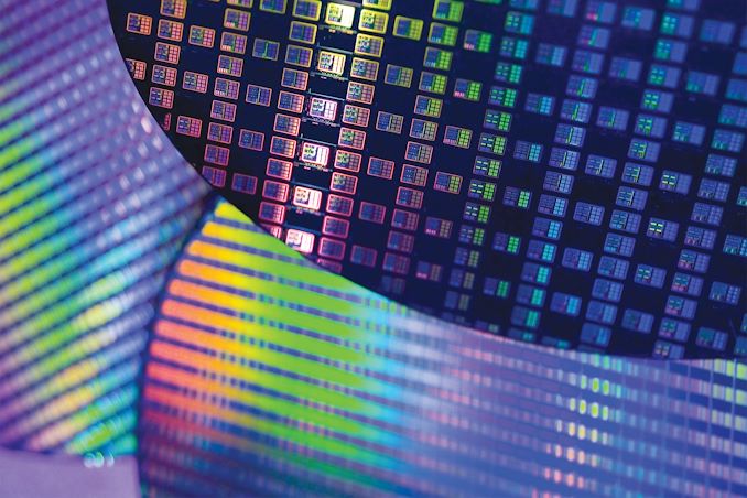
Speaking to partners last week as part of their annual Open Innovation Platform forum in Europe, a big portion of TSMC's roadshow was dedicated to the next generation of the company's foundry technology. TSMC's 2 nm-class N2, N2P, and N2X process technologies are set to introduce multiple innovations, including nanosheet gate-all-around (GAA) transistors, backside power delivery, and super-high-performance metal-insulator-metal (SHPMIM) capacitor over the next few years. But in order to take advantage of these innovations, TSMC warns, chip designers will need to use all-new electronic design automation (EDA), simulation, and verification tools as well as IP. And while making such a big shift is never an easy task, TSMC is bringing some good news to chip designers early-on: even with N2 still a couple of years out, many of the major EDA tools, verification tools, foundation IP, and even analog IP for N2 are already available for use.
"For N2 we could be working with them two years in advance already because nanosheet is different," said Dan Kochpatcharin, Head of Design Infrastructure Management at TSMC, at the OIP 2023 conference in Amsterdam. "[EDA] tools have to be ready, so what the OIP did is to work with them early. We have a huge engineering team to work with the EDA partners, IP partners, [and other] partners."
| Advertised PPA Improvements of New Process Technologies Data announced during conference calls, events, press briefings and press releases |
|||||
| TSMC | |||||
| N5 vs N7 |
N3 vs N5 |
N3E vs N5 |
N2 vs N3E |
||
| Power | -30% | -25-30% | -34% | -25-30% | |
| Performance | +15% | +10-15% | +18% | +10-15% | |
| Chip Density* | ? | ? | ~1.3X | >1.15X | |
| Volume Manufacturing |
Q2 2022 | H2 2022 | Q2/Q3 2023 | H2 2025 | |
*Chip density published by TSMC reflects 'mixed' chip density consisting of 50% logic, 30% SRAM, and 20% analog.
Preparations for the start of N2 chip production, scheduled for sometime in the second half of 2025, began long ago. Nanosheet GAA transistors behave differently than familiar FinFETs, so EDA and other tool and IP makers had to build their products from scratch. This is where TSMC's Open Innovation Platform (OIP) demonstrated its prowess and enabled TSMC's partners to start working on their products well in advance.
By now, major EDA tools from Cadence and Synopsys as well as many tools from Ansys and Siemens EDA have been certified by TSMC, so chip developers can already use them to design chips. Also, EDA software programs from Cadence and Synopsys are ready for analog design migration. Furthermore, Cadence's EDA tools already support N2P's backside power delivery network.
With pre-built IP designs, things are taking a bit longer. TSMC's foundation libraries and IP, including standard cells, GPIO/ESD, PLL, SRAM, and ROM are ready both for mobile and high-performance computing applications. Meanwhile, some PLLs exist in pre-silicon development kits, whereas others are silicon proven. Finally, blocks such as non-volatile memory, interface IP, and even chiplet IP are not yet available - bottlenecking some chip designs - but these blocks in active development or planned for development by companies like Alphawave, Cadence, Credo, eMemory, GUC, and Synopsys, according to a TSMC slide. Ultimately, the ecosystem of tools and libraries for designing 2 nm chips is coming together, but it's not all there quite yet.
"[Developing IP featuring nanosheet transistors] is not harder, but it does take more cycle time, cycle time is a bit longer," said Kochpatcharin. "Some of these IP vendors also need to be trained [because] it is just different. To go from planar [transistor] to FinFET, is not harder, you just need to know how to do the FinFET. [It is] same thing, you just need to know how to do [this]. So, it does take some to be trained, but [when you are trained], it is easy. So that is why we started early."
Although many of the major building blocks for chips are N2-ready, a lot of work still has to be done by many companies before TSMC's 2 nm-class process technologies go into mass production. Large companies, which tend to design (or co-design) IP and development tools themselves are already working on their 2 nm chips, and should be ready with their products by the time mass production starts in 2H 2025. Other players can also fire up their design engines because 2 nm preps are well underway at TSMC and its partners.


20 Comments
View All Comments
my_wing - Sunday, October 15, 2023 - link
Do you know Maths you mentioned 2 years, if ASML provided a High NA scanner to TSMC Q1 2024, then use your primary school Maths, Q2 2024, Q3 2024, Q4 2024, Q1 2025, Q2 2025, Q3 2025, Q4 2026 (test production 1 and half year), then missed iPhone deadline, then Q1 2026, Q2 2026 (ramp) i.e. 2 years, use your figure and count properly.Doug_S - Monday, October 16, 2023 - link
I meant 2-3 years after the initial N2, not 2-3 years from now.my_wing - Monday, October 16, 2023 - link
I can't find the actual link but it was the lady analyst on this showhttps://www.youtube.com/watch?v=CmkUmRM-_uI
She mentioned that TSMC advantage is modular Fab budling, there is no plan, they change when they build, and because
https://technews.tw/2023/09/18/tsmc-n2-gaafet-nano...
This meant that the contractor is not happy and why delay ???
1) Apple did not want their N2 capacity or delay it's requirement.
2) Change the plan and want to switch to high na, remember ASML already promised.
Look at what the news said.
https://www.anandtech.com/show/20044/asml-to-deliv...
"Meanwhile, Samsung Foundry and TSMC are slated to start production of chips on their 2 nm-class nodes (SF2, N2) in late 2025. Though just how High-NA machines factor into their plans remains equally up in the air."
What I am saying is so possible what your 1.4 nm stories is not. Look at fact. There is no love, only money in running a company.
Wereweeb - Sunday, October 15, 2023 - link
N2 isn't a mere node shrink, they're changing the fundamental transistor architecture. They're probably already more than busy enough refining the GAAFET-specific process changes, techniques, design, integration, possibly tooling, etc... where also trying to integrate High-NA into the workflow would end up being counterproductive.Remember that trying to take two steps at a time was how Intel tripped themselves in their 10nm business.
Doug_S - Sunday, October 15, 2023 - link
"Remember that trying to take two steps at a time was how Intel tripped themselves in their 10nm business."Which makes it interesting that TSMC is doing GAAFET alone in N2, and saving backside power for its second iteration (N2P or whatever they call it) Intel meanwhile is attempting GAAFET / "ribbonFET" and backside power at the same time in 20A. If that fails there will be a lot of "I told you sos" from people remembering the 10nm debacle.
Even if they succeed that doesn't mean TSMC should have done both. They have always been conservative - they rolled out N7 without EUV, then a year later introduced N7+ with four EUV layers alongside N7P without EUV, then a year after that introduced N5 with many EUV layers. Doing it that way essentially de-risked the introduction of EUV - if they ran into issues they were still pumping out N7P wafers so they didn't have all their eggs in the EUV basket. But easing into it that way gave them mass production experience with EUV that made N5 their most successful node N5 rollout ever.
my_wing - Monday, October 16, 2023 - link
I really don't see that is the case because I felt like TSMC didn't mastered double patterning using EUV, if yes then iPhone 15 will use N3B, now only pro max, it was also rumor that Apple will only take good chip (due to low yield) as oppose to taking the whole waffle, then TSMC effort is to reduced EUV exposure in N3E, more like they admit defeat, going forward, TSMC N2 has to use double patterning, it deeply depended on what they learned in N3B experience, but the answer seems to be not a lot.I don't see this is that difficult to switch from EUV to EUV NA, it is like I am using Canon then suddenly there is a Hasselblad, or I am driving a Toyota and suddenly there is a Mclaren.
As I mentioned before, the modular Fab building which the Taiwanese so proud of will take care of it then yes they delay the building of Fab in Taiwan is most likely that they change the design (modular) now they just need the time to redesign some aspect to fit the larger EUV NA machine.
At this moment in time they will use EUV to build test chip and once High NA is install they can switch the process using lesser.
The Taiwanese were so proud that they can build a FAB in 18 months, so so so there is no issues to even start a brand new fab for EUV NA today and still meet the Q4 2025 N2 roadmap.
Doug_S - Monday, October 16, 2023 - link
"I don't see this is that difficult to switch from EUV to EUV NA" -- someone with absolutely zero knowledge about how foundries operate.my_wing - Monday, October 16, 2023 - link
You are getting too personal.Reuter don't know, AnandTech don't know so why you come here????
Stop milling idea out of thin air.
https://www.anandtech.com/show/20044/asml-to-deliv...
my_wing - Monday, October 16, 2023 - link
You have no idea as well.You think that my moving to EUV High-NA meant that the whole chip i.e M0-Mx layer all will be EUV High-NA, no way the cost will be insane.
My switching to EUV High-NA knowledgeable person will know that switching to EUV High-NA will meant that M0-M1 will be in High-NA and the rest of the other layer will continue with EUV or even DUV. The cost of exposure is different (power/electricity/depreciation/CAPEX) all different EUV High-NA vs EUV vs DUV.
Yes M0 is the most complex and critical and meant a lot of resource and money is put there, but from a building point of view, you build an extra room right next to the FAB currently build/plan/design to be EUV only, and that extra room like a garage and link the main facility with a rail system that is it. This is what by meant of modular, that garage/module is for M0 so to speak, it done all the nice work in EUV High-NA, then transport to the "older" section of the fab to complete the rest of the layer.
Just a like liver Operation (Brain, heart and liver operation have longer operation hours), the junior doctor is going to perform the opening up of the area, clearing the necessary organ, then the senior doctor (main doctor) going to cut the liver, perform the blood vessel reconstruction, etc. the junior doctor come back to perform the closing up. No only the junior team can learn, but the senior team is not over exhausted on aspect that can be performed by junior. (we are talking about 3-10 hours operation).
Similarly no Fab will use a EUV High NA for work that can be performed by EUV or DUV. Your impossible meant that you think not in the same way as it should be.
ballsystemlord - Thursday, October 26, 2023 - link
@Anton , Don't you have a number by now for chip density of N5 vs N7? N5 has been out for some time now.