AMD Reveals Radeon RX 7900 XTX and 7900 XT: First RDNA 3 Parts To Hit Shelves in December
by Ryan Smith on November 3, 2022 4:46 PM EST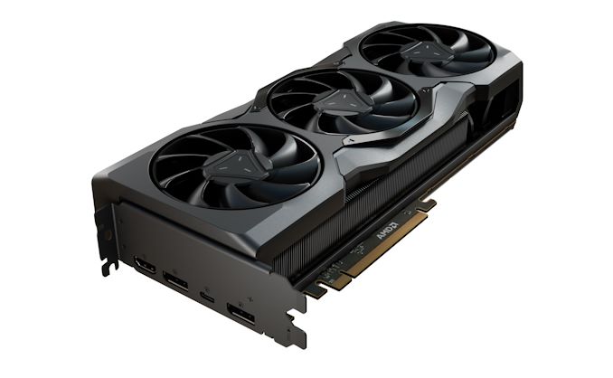
With AMD’s first-wave of Zen 4 CPUs now in the books with the Ryzen 7000 series, the consumer arm of AMD is now shifting its attention over to its graphics business. In a presentation that ended moments ago dubbed “together we advance_gaming”, Dr. Lisa Su and other AMD leaders laid out the future of AMD’s graphics products. And that future is the RDNA 3 architecture, which will be the basis of the new Radeon RX 7900 XTX and Radeon RX 7900 XT video cards.
The two cards, set to be released on December 13th, will be the first products released using the RDNA 3 architecture. According to AMD, the new flagship 7900 XTX will deliver up to 70% more performance at 4K than their previous flagship, the 6950 XT. This performance boost comes curtesy of several architectural improvements in RDNA that cumulatively offer 54% higher performance per watt than RDNA 2, as well as higher clockspeeds courtesy of TSMC’s 5nm (and 6nm) processes, and higher overall power consumption.
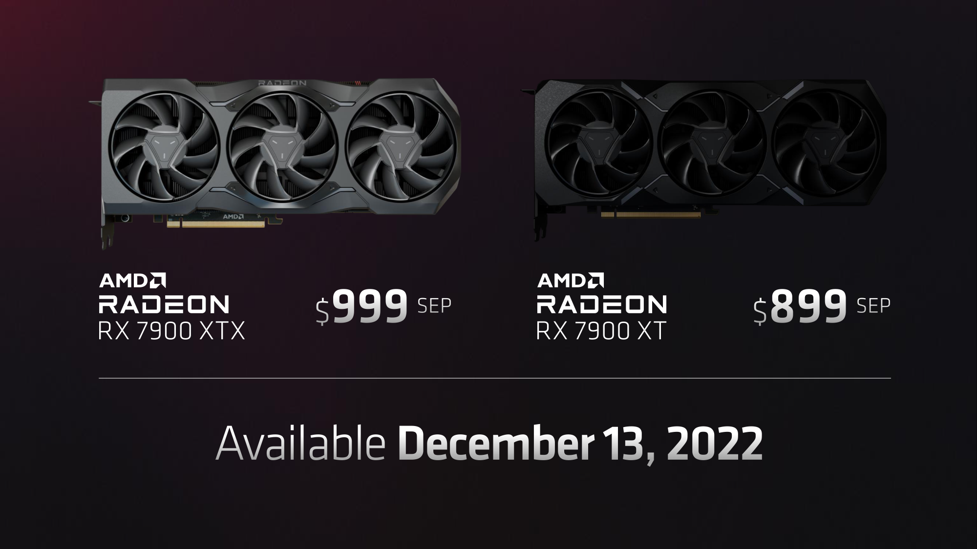
The full-fledged RX 7900 XTX will be hitting the streets at $999. Meanwhile the second-tier RX 7900 XT will run for $899.
| AMD Radeon RX 7000 Series Specification Comparison | ||||||
| AMD Radeon RX 7900 XTX | AMD Radeon RX 7900 XT | AMD Radeon RX 6950 XT | AMD Radeon RX 6900 XT | |||
| Stream Processors | 12288 (96 CUs) |
10752 (84 CUs) |
5120 (80 CUs) |
5120 (80 CUs) |
||
| ROPs | 192 | 192 | 128 | 128 | ||
| Game Clock | 2.3GHz | 2.0GHz | 2100MHz | 2015MHz | ||
| Boost Clock | 2.5GHz | 2.4GHz | 2310MHz | 2250MHz | ||
| Throughput (FP32) | 56.5 TFLOPS | 43 TFLOPS | 21.5 TFLOPS | 20.6 TFLOPS | ||
| Memory Clock | 20 Gbps GDDR6 | 20 Gbps GDDR6 | 18 Gbps GDDR6 | 16 Gbps GDDR6 | ||
| Memory Bus Width | 384-bit | 320-bit | 256-bit | 256-bit | ||
| VRAM | 24GB | 20GB | 16GB | 16GB | ||
| Infinity Cache | 96MB | 80MB | 128MB | 128MB | ||
| Total Board Power | 355W | 300W | 335W | 300W | ||
| Manufacturing Process | GCD: TSMC 5nm MCD: TSMC 6nm |
GCD: TSMC 5nm MCD: TSMC 6nm |
TSMC 7nm | TSMC 7nm | ||
| Transistor Count | 58B | 58B - (1 MCD) | 26.8B | 26.8B | ||
| Architecture | RDNA3 | RDNA3 | RDNA2 | RDNA2 | ||
| GPU | Big Navi 3x | Big Navi 3x | Navi 21 | Navi 21 | ||
| Launch Date | 12/13/2022 | 12/13/2022 | 05/10/2022 | 12/08/2020 | ||
| Launch Price | $999 | $899 | $1099 | $999 | ||
AMD’s eagerly anticipated update to their GPU architecture comes as the company has been firing on all cylinders for the last few years. On the CPU side of matters the Zen 3 and Zen 4 architectures in particular have proven very performant, and meanwhile AMD has been able to claw its way back from its graphics slump with the RDNA family of GPU architectures. RDNA 2, the basis of the Radeon RX 6000 series, exceeded expectations and proved to be a very strong competitor, and now AMD is seemingly setup to exceed expectations once again, with RDNA 3’s 54% performance-per-watt coming in ahead of AMD’s earliest promises of a 50% gain.
AMD Goes Chiplets For GPUs
While today’s reveal from AMD was a more closely guarded event than the Ryzen 7000 unveil a couple of months ago, AMD has still given us a quite a bit of detail on the RDNA 3 architecture and the cards – more than we have time to cover here – so let’s get started from the top, with the construction of the first RDNA 3 GPU.
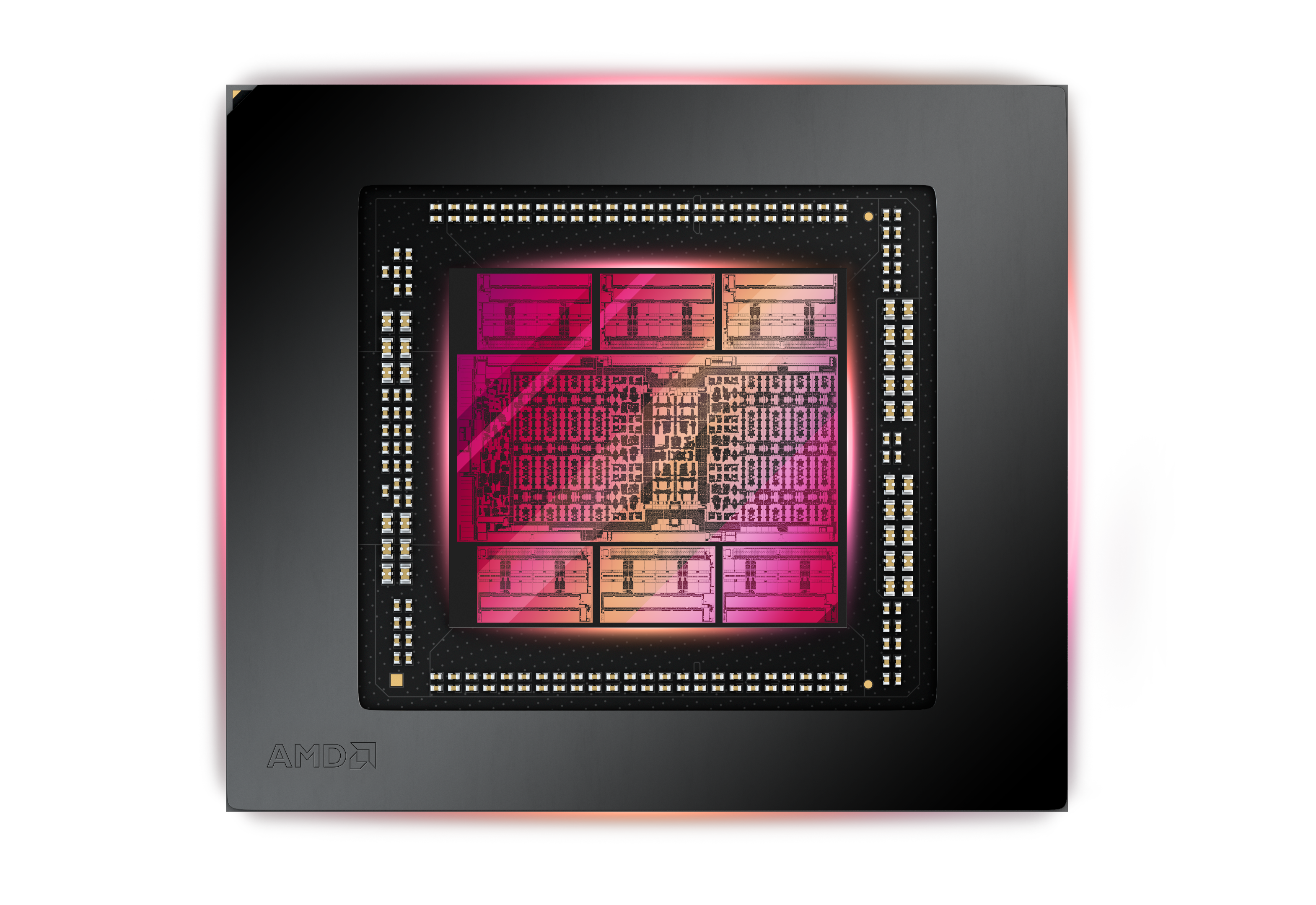
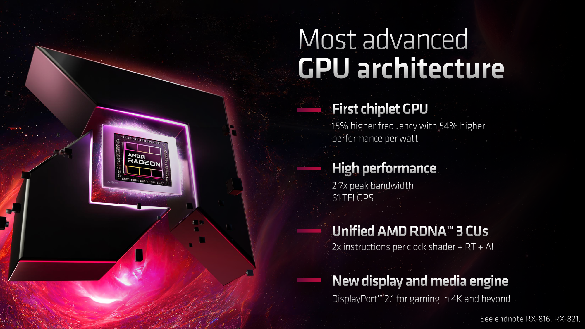
The Navi 3x GPU (AMD is not confirming the specific GPU name at this time) breaks new ground for AMD not only on the performance front, but in terms of its construction. For the first time from any of the big 3 GPU manufacturers, AMD is utilizing chiplets in the construction of the GPU.


Chiplets are in some respects the holy grail of GPU construction, because they give GPU designers options for breaking apart complex monolithic GPU designs into multiple smaller parts – allowing for new options for scaling, as well as mixing and matching the process node used in manufacturing. That said, it’s also a holy grail because the immense amount of data that must be passed between different parts of a GPU (on the order of terabytes per second) is very hard to do – and very necessary to do if you want a multi-chip GPU to be able to present itself as a single device.
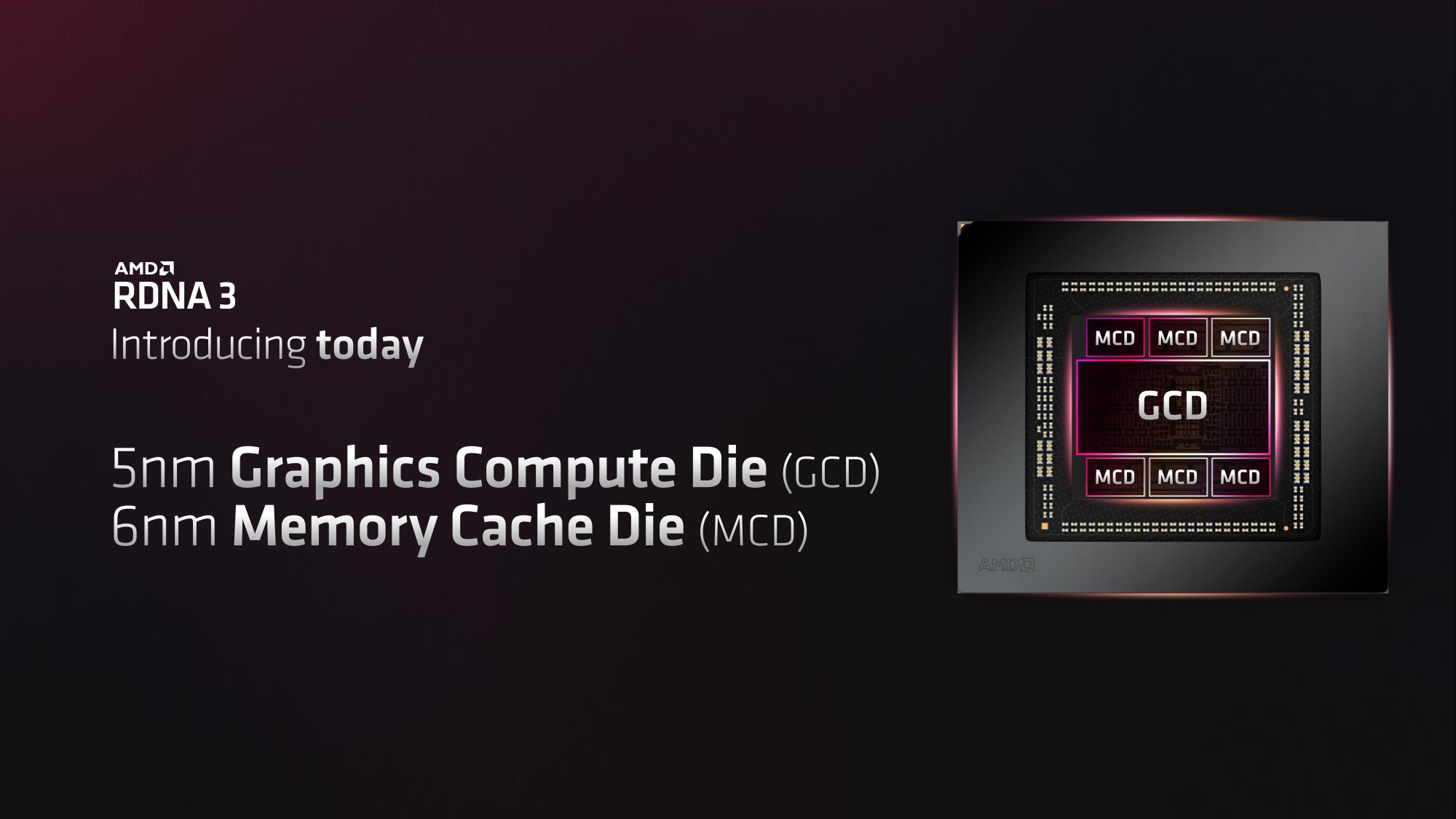
For their big Navi 3x chip, AMD has assembled two types of chiplets, essentially breaking off the memory functions from a classic GPU into their own chiplets. This means that the core functions of the GPU are housed in what AMD is calling the Graphics Compute Die (GCD), which houses all of the ALU/compute hardware, the graphics hardware, as well as ancillary blocks like the display and media engines.
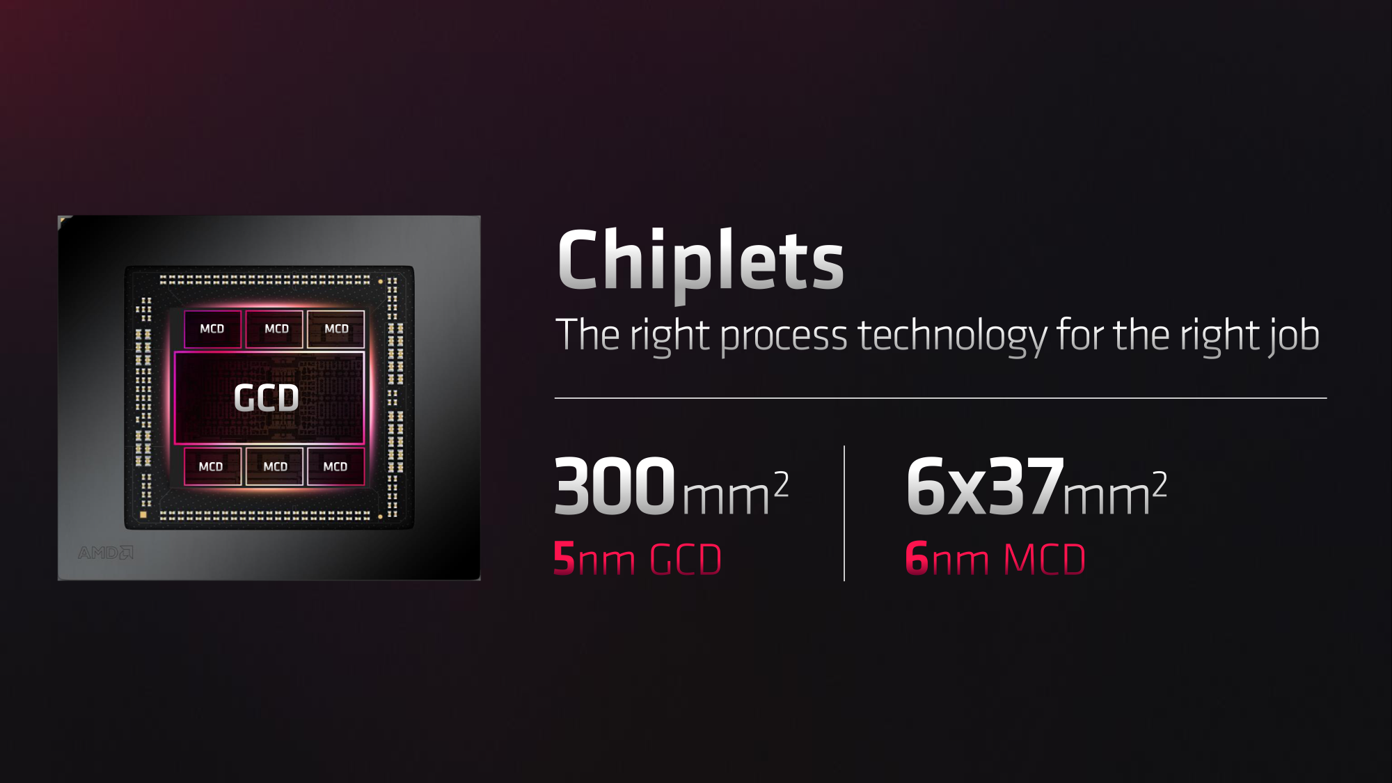
Because the GCD houses the performance-critical aspects of the overall GPU, it’s being built on TSMC’s 5nm process. This gives AMD the best density, power consumption, and clockspeeds for these parts, though obviously at a higher manufacturing cost. The GCD die size measures 300mm2.
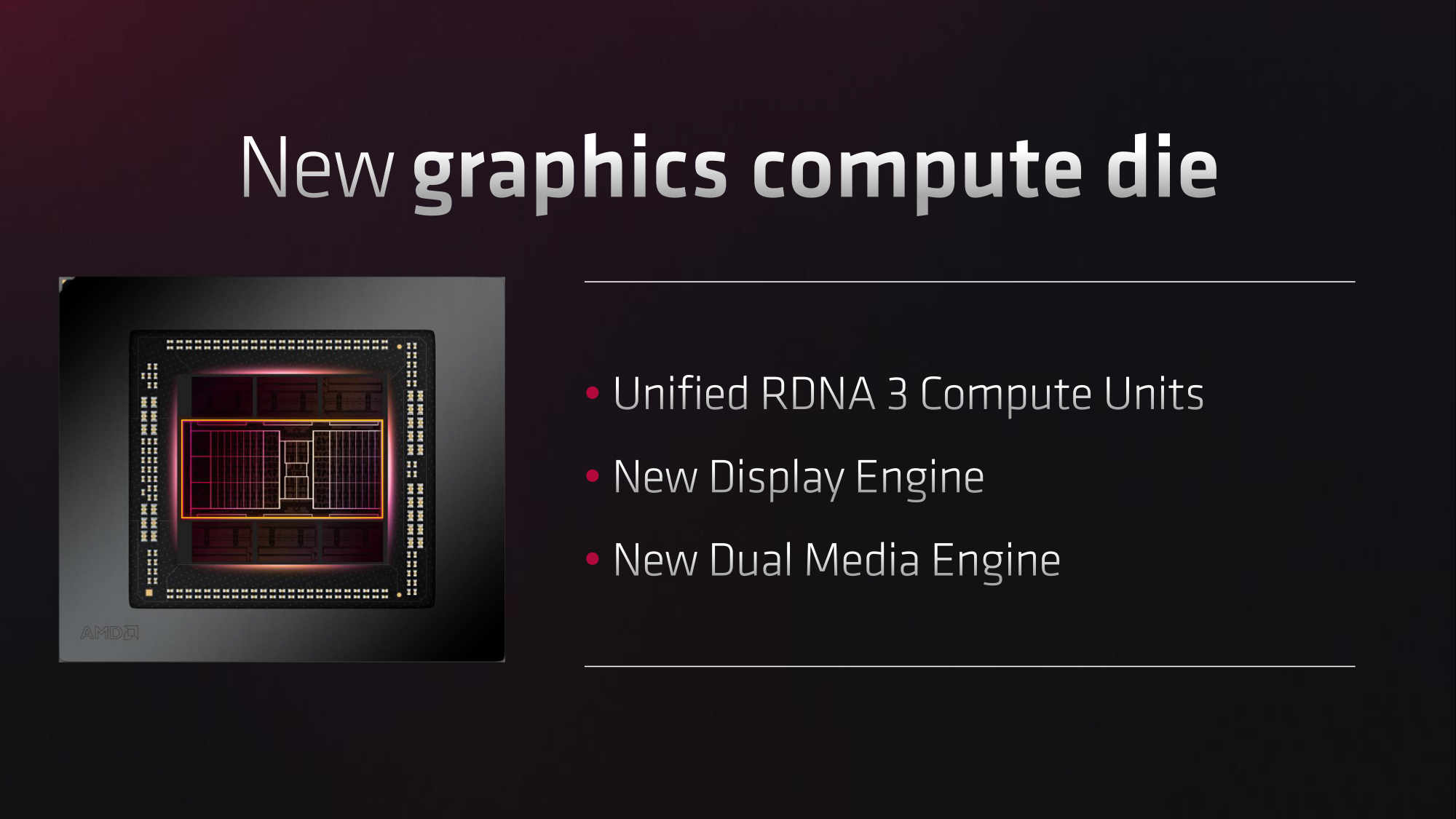
Meanwhile the new Memory Cache Die (MCD) houses AMD’s infinity cache (L3 cache), as well as a 64-bit (technically 2x32-bit) GDDR6 memory controllers. The MCD is one of the scalable aspects of the chiplet design, as Big Navi 3x GPU SKUs can be configured by paring them with more or fewer MCDs. A full configuration in this case is 6 active MCDs, which is what we see in the 7900 XTX. Meanwhile the 7900 XT will have 5 active MCDs, with a 6th defective/spacer MCD present for salvaging purposes and physical package stability.
An individual MCD is 37mm2 in die size, and is built on TSMC’s 6nm process. This is an example of AMD’s process node flexibility, putting the less critical GDDR6 memory controllers and Infinity Cache on a cheaper process node. GDDR6 controllers are one of those classic examples of a technology that doesn’t scale very well with smaller process geometries (like most forms of I/O), so it’s easy to see why AMD would want to avoid building it on 5nm for minimal benefits.
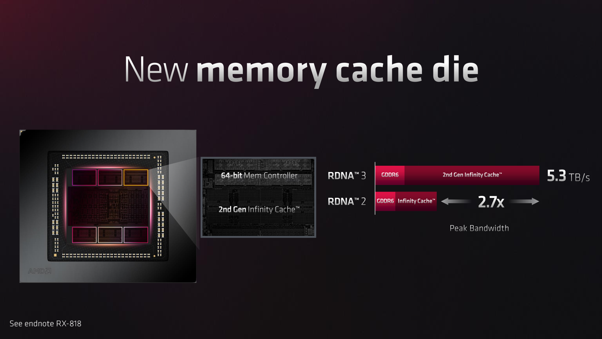
In the full 6 MCD configuration (7900 XTX), Big Navi 3x offers a 384-bit GDDR6 memory bus, along with 96MB of L3 cache. Meanwhile a 5 MCD (7900 XT) offers a 320-bit GDDR6 memory bus and 80MB of L3 cache.
For the purposes of today’s announcement, AMD has not gone into great depth on how they managed to make a chiplet-based GPU work, but they have confirmed a few important details. First and foremost, in order to offer the die-to-die bandwidth needed have the memory subsystem located off-chip, AMD is using an unspecified fanout bridge technology. their Elevated Fanout Bridge (EFB) packaging technology, which AMD first used for their Instinct MI200 series accelerators (CDNA2). On those accelerator parts it was used to hook up the monolithic GPUs to each other, as well as HBM2e memory. On RDNA 3, it’s being used to hook up the MCDs to the GCD.
Notably, fanout bridges are a non-organic packaging technology, which is to say it’s complex. That AMD is able to get 5.3TB/second of die-to-die bandwidth via it underscores its utility, but it also means that AMD is undoubtedly paying a good deal more for packaging on Big Navi 3x than they were on Navi 21 (or Ryzen 7000).
Internally, AMD is calling this memory-to-graphics link Infinity Link. Which, as the name implies, is responsible for (transparently) routing AMD’s Infinity Fabric between dies.
As mentioned before, the cumulative bandwidth here between the MCDs and GCD is 5.3TB/second. It’s unclear if the constraining factor is the bandwidth of the Infinity Link, or that the combined Infinity Cache + GDDR6 memory controllers cannot move enough data to fully saturate the link. But regardless, it means there’s essentially just shy of 900GB/second of bandwidth between an individual MCD and GCD – more than all of the combined off-die memory bandwidth of the last-generation Radeon RX 6950 XT (and 2.7x more than Navi 21’s on-die bandwidth).
While we’re on the subject of AMD’s L3 Infinity Cache, it’s notable here that it’s actually a bit smaller on Big Navi 3x than it was on Navi 21, with a maximum capacity of 96MB versus 128MB on the former. According to AMD they’ve made further improvements to improve data reuse on the Infinity Cache to offset this drop in capacity. At this point it’s not clear if the change is a function of software algorithms, or if they’ve made more fundamental hardware changes.
Finally, while AMD is quoting die sizes for the GCD and MCD, they aren’t quoting individual transistor counts. So while we know that a complete 6 MCD Big Navi 3x configuration is comprised of 58 billion transistors (2.16x more than Navi 21), we don’t know how much of that is the GCD versus the MCDs.

AMD RDNA 3 Compute & Graphics Architecture: Bringing Back ILP & Improving RT
Diving down a level, let’s take a look at the actual graphics and compute architecture backing RDNA 3 and Big Navi 3x.
While still clearly sharing many of the core design elements of AMD’s overarching RDNA architecture, RDNA 3 is in some respects a much bigger shift in architectural design than RDNA 2 was. Whereas RDNA 2’s compute core was essentially unchanged from RDNA (1)’s, RDNA 3 makes a few big changes.
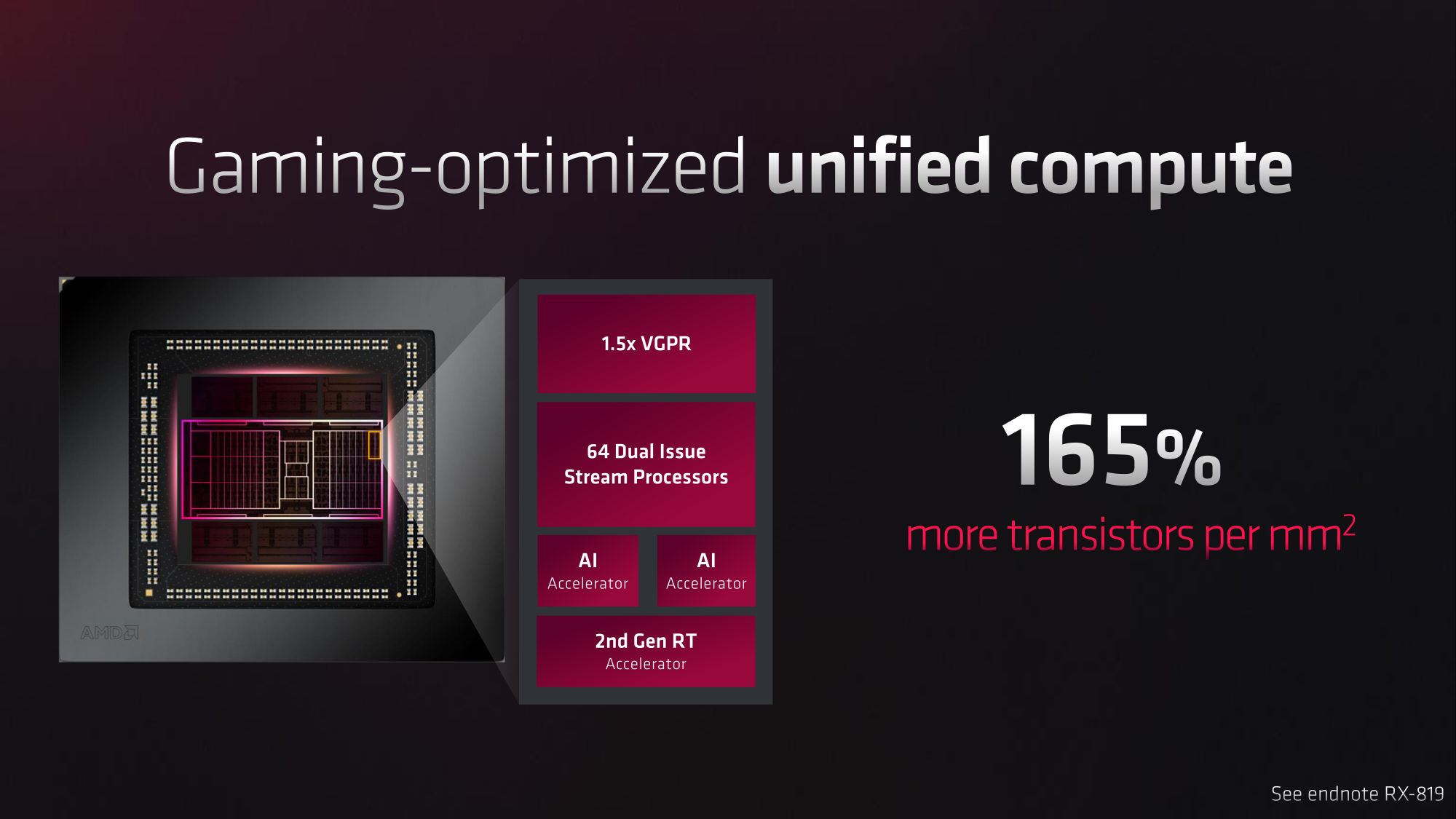
The biggest impact is how AMD is organizing their ALUs. In short, AMD has doubled the number of ALUs (Stream Processors) within a CU, going from 64 ALUs in a single Dual Compute Unit to 128 inside the same unit. AMD is accomplishing this not by doubling up on the Dual Compute Units, but instead by giving the Dual Compute Units the ability to dual-issue instructions. In short, each SIMD lane can now execute up to two instructions per cycle.
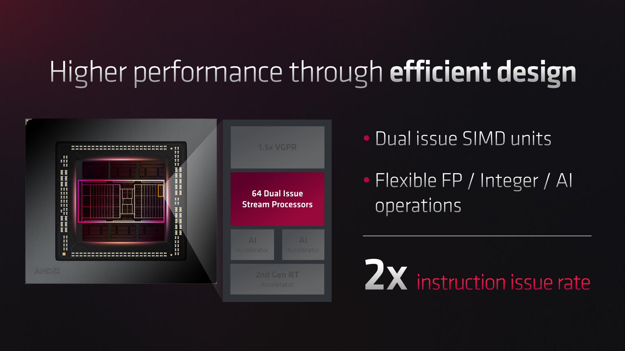
But, as with all dual-issue configurations, there is a trade-off involved. The SIMDs can only issue a second instruction when AMD’s hardware and software can extract a second instruction from the current wavefront. This means that RDNA 3 is now explicitly reliant on extracting Instruction Level Parallelism (ILP) from wavefronts in order to hit maximum utilization. If the next instruction in a wavefront cannot be executed in parallel with the current instruction, then those additional ALUs will go unfilled.
This is a notable change because AMD developed RDNA (1) in part to get away from a reliance on ILP, which was identified as a weakness of GCN – which was why AMD’s real-world throughput was not as fast as their on-paper FLOPS numbers would indicated. So AMD has, in some respects, walked backwards on that change by re-introducing an ILP dependence.
We’re still waiting on more information from AMD outlining why they made this change. But dual-issue is typically a cheap way to add more throughput to a processor design (you don’t have to do all the instruction tracking required for a fully separate Dual Compute Unit), and it can be worthwhile tradeoff if you can ensure you’ll be able to dual-issue most of the time. But it means that AMD’s real-world ALU utilization rate is likely lower on RDNA 3 than RDNA 2, due to the bubbles from not being able to dual-issue.
Which to bring things back to gaming and the products at hand, it means that the FLOPS numbers between RDNA 3 and RDNA 2 parts are not going to be entirely comparable. 7900 XTX may push 2.6x as many FP32 FLOPs as 6950 XTX on paper, but the real world advantage on anything less than ideal code is going to be less. Which is one of the reasons why AMD is only promoting a real-world performance uplift of 1.7x for the 7900 XTX.
In any case, SIMDs aren’t the only changes to the core compute architecture of RDNA 3. Feeding the beast, AMD has made the Vector General Purpose Register (VGPR) bank 50% larger than on RDNA 2.
More significant than that is that AMD is finally integrating dedicated silicon for AI processing on their consumer GPUs. This is an area where both of AMD’s competitors (NVIDIA and Intel) have already made the investment on their consumer parts, and as the use of GPU inference in workloads continues to grow, it’s not something AMD can ignore any longer.

Given the gaming-centric focus of today’s presentation, AMD did not spend much time talking about the new AI units. Each RDNA 3 CU will have 2 of these units, and they will support new AI instructions (some kind of INT8 tensor operation seems like a given). All told, AMD is saying that the new AI units give the Radeon RX 7900 XTX 2.7x the AI performance, which AMD is measuring as bfloat16 performance versus the RX 6950 XT.
Overall, the importance of this to gamers is something that remains to be seen. AMD isn’t currently using AI units for FSR 2 (unlike NVIDIA’s DLSS 2). But that could change for future projects. Otherwise, for more professional users (or anyone who likes to mess with Stable Diffusion), this is an addition that’s good news.
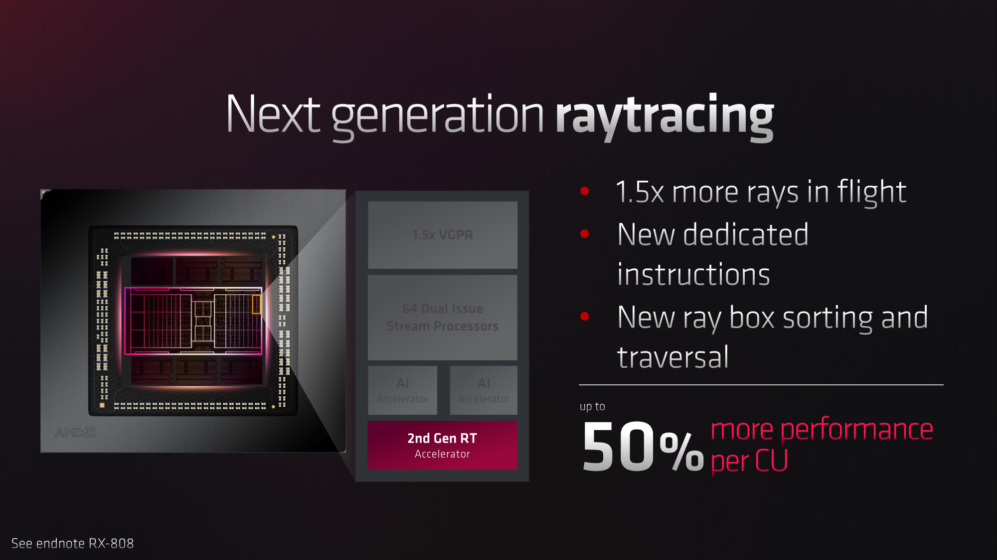
Moving on, AMD has also updated their raytracing hardware for RDNA 3. The second-generation RT accelerator, as AMD calls it, can handle 1.5x more rays in flight. There are also new hardware box sorting and traversal features that weren’t present in RDNA 2’s initial RT functionality. AMD’s presentation gave the technical details a light treatment, but it certainly looks like AMD is moving to doing a bigger part of the ray tracing process in dedicated hardware. Which in turn would help improve their performance, and keep performance steadier by not stealing quite so many resources from the rest of the CU.
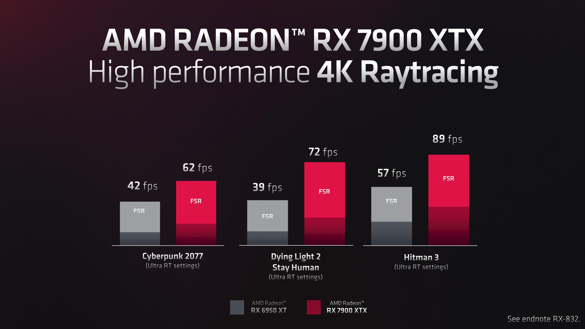
AMD’s own performance slides tout anywhere between a 47% and 84% increase in RT performance. Though it should be noted that AMD’s numbers are with FSR enabled; so we cannot divorce these gains from any changes that improve FSR performance on the 7900 XTX.
Last, but not least, AMD has made an interesting decision with clockspeeds on the RDNA 3. In short, AMD has decoupled their clocks; rather than running the entire GCD at the same clockspeed, AMD will be running the shaders and front-end at different clockspeeds. In the case of the 7900 XTX, this will see the shaders running at 2.3GHz (the advertised game clock speed), while the front-end will run at a slightly speedier 2.5GHz (about 9% faster).
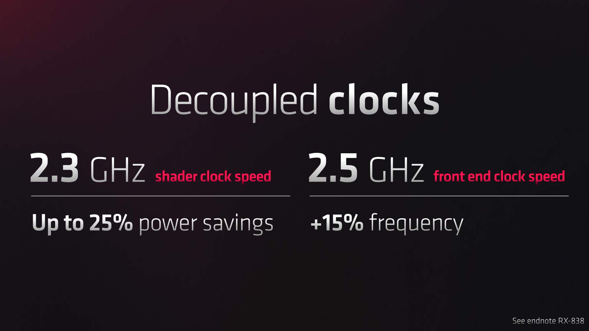
AMD did not go into great detail on why they’ve made this change, but at a high level it’s all about balancing performance versus power consumption. The shaders could run at 2.5GHz as well (indeed, the 7900 XTX’s rated boost clock is 2.5GHz), but as we’ve seen time and time again, those final clocks are the most expensive in terms of power as you go up the v/f curve. So AMD has made the choice to give up a bit of potential performance to save a lot on power, as 96 CUs/12288 ALUs is a lot of silicon to light up. Conversely, the front-end is relatively small, and with AMD having beefed up their CUs by so much, spending a bit more power on the front-end is presumably worth it to keep them from bottlenecking the rest of the GPU.
RDNA 3 Display & Media Engines: The Latest and the Greatest
AMD’s core compute/graphics architecture was not the only part of the RDNA 3 architecture to get an update in this generation. AMD has also used the opportunity to upgrade their display and media engines to support new features and new formats.
On the display engine front, AMD’s display engine, which they are now calling the “AMD Radiance Display Engine” has been upgraded to support DisplayPort 2.1. Specifically, AMD has added support for the DisplayPort 2.x feature suite as well as the UHBR 10 and UHBR 13.5 data rates. This means that RDNA 3 cards can offer 2x the DisplayPort bandwidth of their DisplayPort 1.4-enabled predecessors, which in turn allows for higher resolutions and higher refresh rates. Notably, this ever so slightly exceeds HDMI 2.1’s bandwidth as well, putting DisplayPort back into the lead, at least on AMD cards.
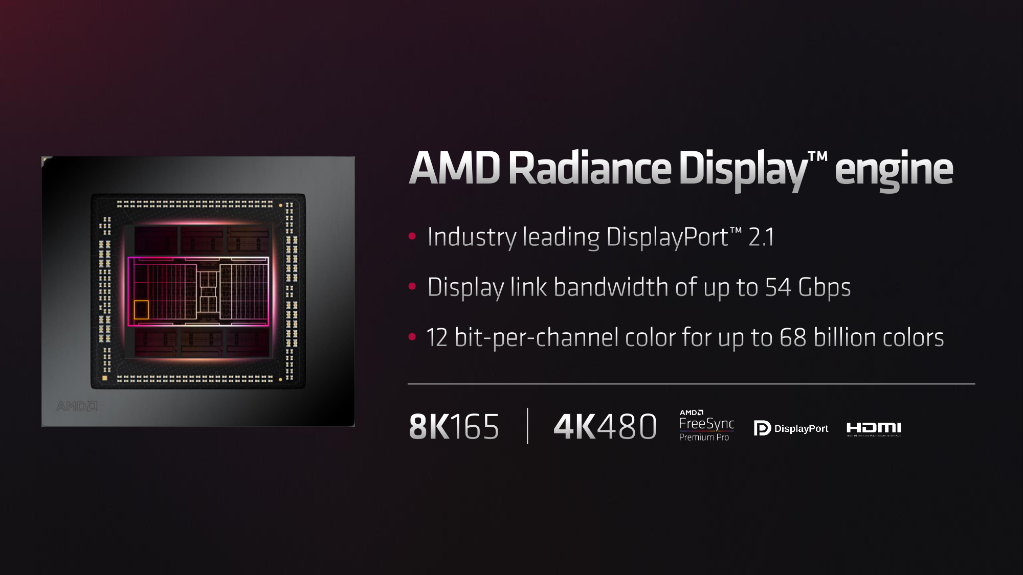
Unsurprisingly, AMD is using this functionality to push forthcoming higher resolution and higher refresh rate gaming monitors, including a Samsung ultrawide display set to launch in 2023 with a horizonal 8K resolution. So it’s not just for showing off specs, and AMD and its partners are intending to put it to good use.

AMD has not said anything about the total number of supported displays. So at this point I expect it’s still a maximum of 4 displays.
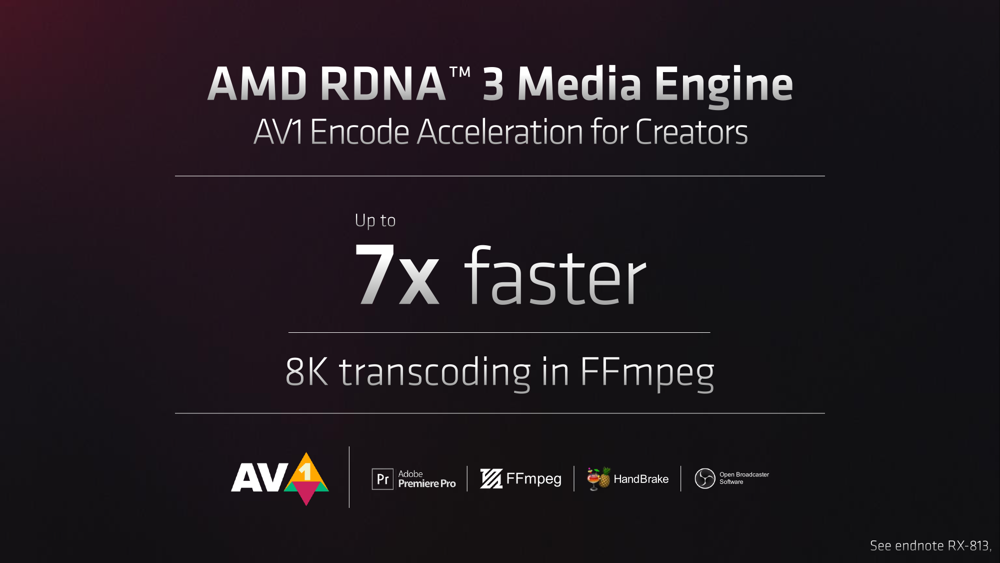
Meanwhile on the media engine front, AMD has given RDNA 3 support for the latest and greatest video codecs. Along with the usual H.264 and H.265 support, RDNA 3’s media engines also add full AV1 encode and decode support, making this the latest GPU family to roll out support for the next-generation open format codec. RDNA 3 will be able to encode and decode AV1 at up to 8Kp60.
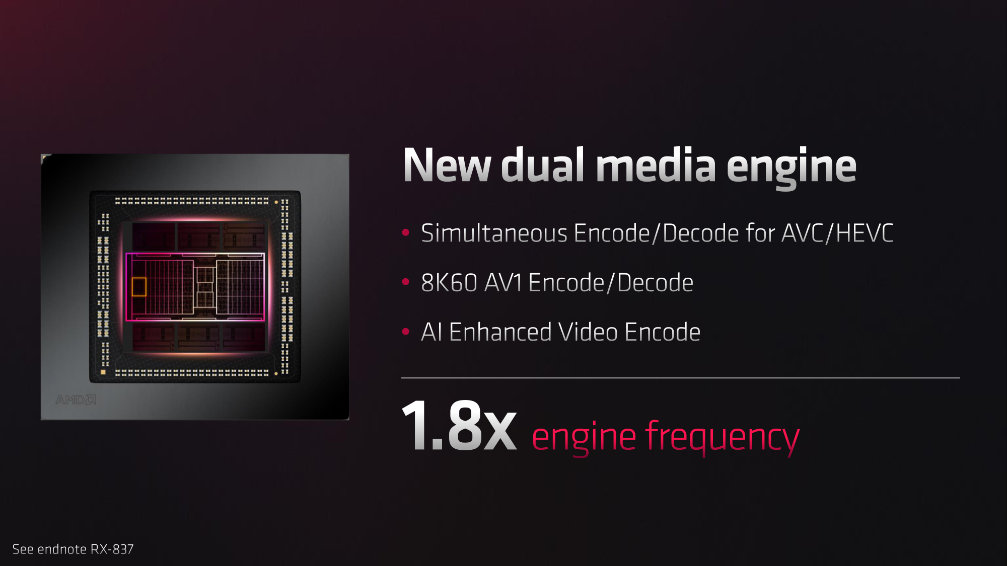
The overall performance of the media engine has been increased significantly. According to AMD the media engine runs 80% faster than it did on RDNA 2 parts, allowing for simultaneous encoding (or decoding) of up to two H.264/H.265 streams. Though it’s unclear if that also applies to AV1.
Finally on the subject of AMD’s GPU uncore, while not explicitly called out in AMD’s presentation, it’s worth noting that AMD has not updated their PCIe controller. So RDNA 3 still maxes out at PCIe 4.0 speeds, with Big Navi 3x offering the usual 16 lanes. This means that even though AMD’s latest Ryzen platform supports PCIe 5.0 for graphics (and other PCIe cards), their video cards won’t be reciprocating in this generation. In fact, this means that no one will have a PCIe 5.0 consumer video card.
Radeon RX 7900 XTX & Radeon RX 7900 XT: Launching December 13th
Bringing today’s reveal full circle, let’s turn back to the cards themselves, the Radeon RX 7900 XTX and RX 7900 XT.
AMD’s flagship card will be the Radeon RX 7900 XTX. While we’re still waiting on confirmation of this, this would seem to be a fully-enabled Big Navi 3x part, with all of the blocks in both the GCDs and the individual MCDs themselves enabled. As mentioned previously, AMD is touting a broad performance uplift of up to 70% versus the previous-generation flagship, the RX 6950 XT.
Internally, this means 96CUs and 96MB of L3 Infinity Cache will be available on the card. The game clock (average clockspeed) will be 2.3GHz, while based on other AMD figures, we can infer that the boost (maximum) clockspeed will be 2.5GHz. The game clock in particular is a ~10% improvement over the 6950 XT, so AMD is enjoying a modest frequency uplift generation-over-generation, but nothing too massive. Most of the heavy lifting will come courtesy of the architecture and memory changes.


Speaking of memory, the RX 7900 XTX will be paired with 24GB of GDDR6 memory running at (at least) 20Gbps. Apparently, AMD’s partners have the headroom to go even higher than this with factory overclocking, but the floor value for the part will be 20Gbps overall. This is a modest increase in memory clockspeeds versus the 6950 XT (11%). Instead, the bulk of the VRAM bandwidth gains will come from the 50% larger memory bus, with the 7900 XTX moving to a sizable 384-bit bus. In total, this means the 7900 XTX will have 960GB/sec of memory bandwidth, 66% more than its predecessor. AMD got their “free” memory subsystem performance boost in the last generation with Infinity Cache, so for this time around, they are back to needing to add more physical memory bandwidth to keep the ever-growing beast properly fed.
Meanwhile, the 7900 XT will be a chip off the block, with fewer CUs, less VRAM, and lower clockspeeds. All told we’re looking at 84CUs paired with 20GB of 20Gbps GDDR6, and backed by an 80MB infinity cache. The card’s game clockspeed rating is 2.0GHz, and we do not have any information on the boost clockspeed. The combination of a 13% drop in clockspeeds and 13% drop in CUs adds up to what is, on paper, a 24% deficit in compute/shading performance. That said, AMD’s pricing indicates that the real-world performance gap shouldn’t be this high, and we’re still missing some important details such as ROP counts. So for better or worse, we don’t have a good frame of reference fright now for how the 7900 XT will perform relative to anything else, current-generation or last.


Unsurprisingly, power consumption at the high end will be going up. The 7900 XTX will be a 355W card, up 20W from the 335W 6950 XT (and 55W from the 300W 6900 XT). This is a more modest power requirement than on NVIDIA’s high-end RTX 4090 Ti (450W), but we’re still talking about a card well north of 300W. For gamers with a slightly smaller appetite for large power bills, the 7900 XT will be holding the line at 300W. Both cards will require 2 8-pin PCIe power connectors.
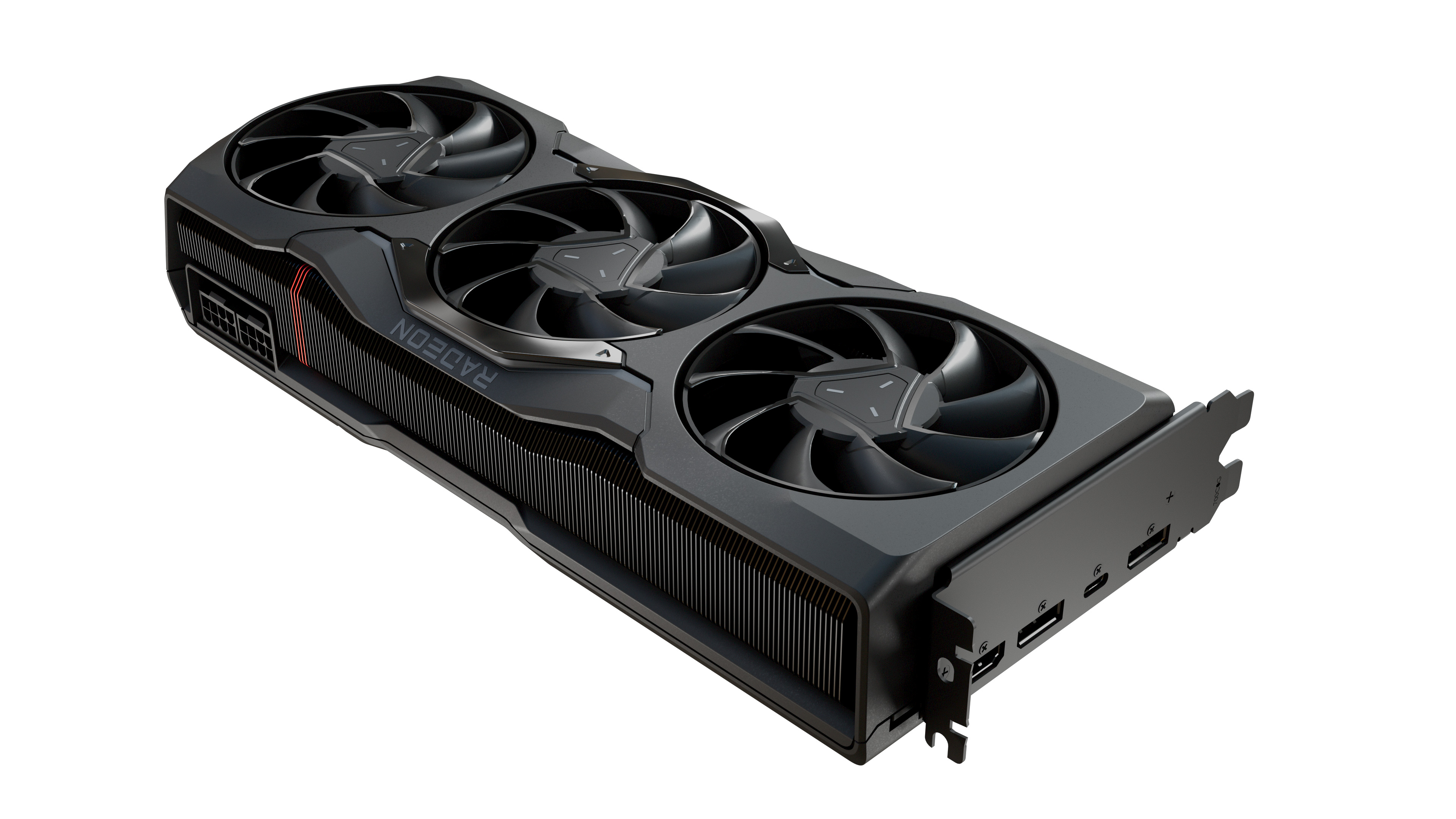
AMD has also sent over pictures of both the reference 7900 XTX and 7900 XT. Of particular note, both cards will feature a USB-C port for display outputs. This is a feature that AMD introduced with the RX 6000 series and has opted to carry forward into the RX 7000 series. As with the previous-gen cards, the presence of the USB-C port is for directly hooking up monitors that rely on DisplayPort Alt Mode over USB-C. Meanwhile, rounding out the collection will be a paid of DisplayPorts (2.1) and an HDMI 2.1 port.
Both cards are using a new triple fan blower design from AMD. We’re still waiting on further details here, but AMD has told us that the 7900 XTX measures 287mm long, and is 2.5 slots wide.
Wrapping things up, both cards will be launching on December 13th, with AMD planning on having both reference and AIB partners’ cards on the shelf for launch day. The 7900 XTX will start at $999, meanwhile the 7900 XT will be right behind it at $899. AMD isn’t offering any performance comparisons versus NVIDIA cards, but at this juncture it seems like the wildcard is the soon-to-launch GeForce RTX 4080 16GB. By the time AMD launches in December, we should have a much better idea of where AMD and NVIDIA’s dueling lineups stand in comparison to each other.


197 Comments
View All Comments
Khanan - Sunday, November 13, 2022 - link
Not since RX 6000 Gen, their “made by amd” cards are actually pretty decent, have good acoustics, good cooling.evolucion8 - Thursday, November 10, 2022 - link
I recall that GCN was actually a TLP design, not ILP design like Evergreen and the Terascale architecture in previous generations. I think the issue with GCN was that the hardware schedule wasn't able to scale as well when going beyond 11 CUs due to internal architectural bottlenecks with instruction issue, internal bandwdith and the 4 shader per SE.RDNA 1 and 2 are convincingly TLP designs and moving away to a ILP design would require a major redesign of the compiler and the ISA language (RDNA can run under Wave64 used on GCN), so I doubt they would risk such a risky move as it means that their design would require some optimizations which would be from scratch. (Unless if this design keeps the Wave32 approach, or goes into Wave64 approach like GCN).
Khanan - Thursday, November 10, 2022 - link
The issue was that GCN forced Wave64 while RDNA and successors can do 32, aside from other optimizations and a more balanced architecture with more ROPs. GCN was simply not optimized for gaming while RDNA is.evolucion8 - Thursday, November 10, 2022 - link
Wave64 would leave too much bubbles but each SIMD was 64 instructions wide, couldn't take 32 like RDNA. GCN also had a terrible geometry bottleneck which only got fixed with Vega somewhat lol.occidental - Sunday, December 11, 2022 - link
Love to mate the XTX with my 7950X, currently sharing space with an Nvidia RTX A4000. However, I need vMix, Davinci Resolve Studio and OBS to properly leverage the encoders in the XTX, at launch. My life is high end corporate streaming and video editing, and a 4080 currently flies on all of my use cases. An extra $500 on a 4080, saves me $1000-2000/month in saved time rendering out 4k and greater footage.ryanhill - Tuesday, December 13, 2022 - link
Wow, I thought it will be more expensiveShmee - Saturday, December 24, 2022 - link
So, how about them reviews? :P