Bringing Geek Back: Q&A with Intel CEO Pat Gelsinger
by Dr. Ian Cutress on October 29, 2021 11:30 AM EST
One of the overriding key themes of Pat Gelsinger’s ten-month tenure at Intel has been the eponymous will to ‘bring geek back’ to the company, implying a return to Intel’s competitive past which relied on the expertise of its engineers to develop market-leading products. During this time, Pat has showcased Intel’s IDM 2.0 strategy, leveraging internal production, external production, and an update to Intel’s foundry offering, making it a cornerstone of Intel’s next decade of growth. The first major launch of this decade happened this week, at Intel’s Innovation event, with the announcement of 12th Gen Core, as well as updates to Intel’s software strategy up and down the company.
After the event, Intel invited several media and an analyst or two onto a group session with CEO Pat, along with CTO Greg Lavender, a recent new CTO hire coming from Pat’s old stomping ground at VMWare. In light of the announcements made at Intel Innovation, as well as the financial quarterly results released just the week prior, and the state of the semiconductor supply globally, everyone had Intel at the forefront of their minds, ready to ask for details on Intel’s plan. Each person got the chance to ask a single question in the 30-minute session, although with a couple of minutes at the end, I managed to ask a second.
Pat Gelsinger CEO |
Greg Lavender CTO |
The following is a tidied-up transcript.
Dan Hutchinson, VLSI Research: You've been talking a lot about IDM 2.0 – I like the concept. But what is it that makes it different from ‘IDM 1.0’ that elevates it above buzzword status? [I preface this] In the sense of the belief I've come to that ‘IDM fabless’/fab-light concepts are really just distinctions with very little difference.
Pat Gelsinger: For us, when we talk about IDM 2.0, we talk about three legs. One is a recommitment to IDM 1.0, and Intel’s design and manufacturing at scale. Second is the broad leveraging of the foundry ecosystem. Third, and most importantly, is becoming a foundry, and swinging the doors of Intel Fabs, our packaging, and our technology portfolio - being wide-open to engage with the industry to design on our platforms with our IP. It also involves opening up the x86 architecture, as well as all of the other IP blocks, graphics, IO, memory, and others. By adding second element, but most importantly the third element of that, to me is what makes IDM 2.0.
The other thing I'd add to that, Dan, is that I use this language inside and outside the company: IDM makes IFS better, and IFS makes IDM better. IFS meaning our Intel Foundry Services. In a quick example of both, for IDM, my foundry customers get to leverage all of the R&D and IP that I'm creating through my internal design. Normally foundries have to go create all of that, but Intel can leverage the 10s of billions of capital, many billions of R&D, and the most advanced components research on the planet. It’s essentially for free to my foundry customers. It’s an extraordinary asset. That includes making x86 and other design blocks available for foundry customers. At the same time, Foundry is driving us to do a better job in IDM. We're engaging with a third-party IP ecosystem more aggressively, and with the EDA tool vendors more aggressively. For instance, our engagement with Qualcomm - they're driving us to do a more aggressive optimization for power and performance, more than our more performance-centric product lines would be. So they're making IDM better by the engagement with IFS customers. Standardized PDKs, and other things. So, IDM and IFS, if this really gets rolling as I'm envisioning it to be, they're powerfully going to be reinforcing each other.
Timothy Prickett Morgan, The Next Platform: I'm trying to understand the new Aurora system: the original machine was supposed to be north of [an exaflop] and $500 million. Now it's two Exaflops, or in excess of two Exaflops, and you've got a $300 million write-off for federal systems coming in the fourth quarter. Is that a write-off of the original investment, or is Argonne getting the deal of the century on a two [exaflop] machine?
PG: [Since] the original concept of Aurora, we've had some redefinitions of the timelines and the specifications associated with the project efforts. Obviously some of those earlier dates when we first started talking about the Aurora project we've moved out and changed the timelines for a variety of reasons to get there. Some of those changes lead to the write-off that we're announcing right now. The way the contract is structured, part of it is that the moment that we deliver a certain thing, we will incur some of these write-offs simply from the accounting rules associated with it. As we start delivering it, some of those will likely get reversed next year as we start ramping up the yields of the products. So some of it just ends up being how we account for and how the contracts were structured.
On the two versus one Exaflop: largely it’s PVC, you know, Ponte Vecchio. The core of the machine is outperforming the original contractual milestones. So when we set it up to have a certain number of processors, and you can go do the math of what two [Exaflop] is, we essentially overbuilt the number of sockets required to comfortably exceed one Exaflop. Now that PVC is coming in well ahead of those performance objectives for some of the workloads that are in the contract, we're now comfortably over two Exaflop. That's pretty exciting at that point - that we will go from one to two pretty fast.
But to me, the other thing that's really exciting in this space is our Zetta Initiative. What we've said is that we're going to be the first to Zettascale by a wide margin. We're laying out as part of the Zetta initiative what we have to do in the processor, in the fabric, in the interconnect and the memory architecture, what we have to do for accelerators, and the software architecture to do it. So Zettascale in 2027 – it’s a huge internal initiative that's going to bring many of our technologies together for a 1000x gain in five years. That's pretty phenomenal.

Ian Cutress, AnandTech: Earlier in the year, as part of this IDM 2.0 initiative, one of the big announcements was a collaboration with IBM. IBM is obviously big in the field, with lots of manufacturing and research expertise. We were promised more color on that partnership by the end of the year - is there any chance you can provide that color today?
PG: I don't have a whole lot more to say, but let me just characterize it a little bit. It's one of the things I think you will be hearing more from us before the year is out. But basically, we're partnering with IBM - think of them as another components research partner with us, in advanced semiconductor research, as well as in advanced packaging research. We're partnering with IBM in those areas. Also, IBM is looking for a partner as well on their manufacturing initiatives, and what they require for their products and product lines. We're aligning together on many of the proposals that you've seen, such as the Ramp-C proposal that we were just granted. Phase one of that involves IBM partnering with us in those areas, so it’s a fairly broad relationship. You'll be hearing more from us before the year-end I expect.
Mark Hachman, PCWorld: I have a very simple, high-level manufacturing question. Your new statement is about keeping up, or superseding Moore's law, over the next decade. Is this something that you think is going to be unique to Intel, or do you think your competitors will also keep pace?
PG: I described four things today that I think enable us to go ‘at Moore's Law’ or ‘Super Moore's Law’.
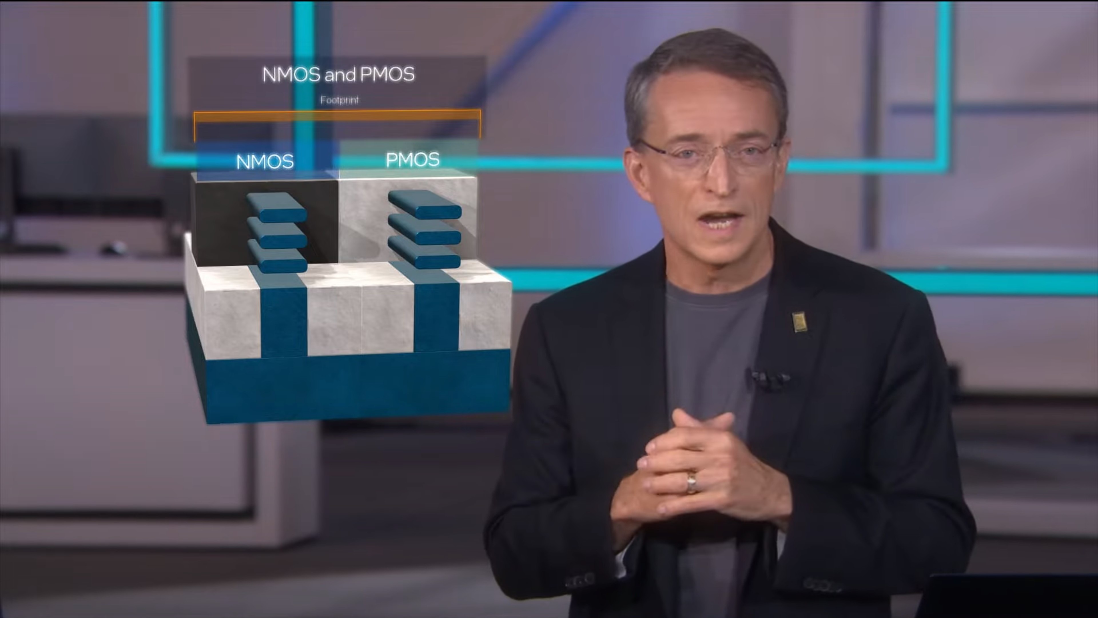
I said EUV, and EUV’s obviously available to the industry, but we're going to be advantaged at High-NA (Intel has stated it will be first to High-NA EUV with ASML). It’s the second generation of EUV. We also talked about RibbonFETs, the fundamental new transistor architecture. As we look at where we are versus others, we think we're comfortably ahead of anybody else with our Gate-All-Around structure that we'll be putting into mass manufacturing in 2024. So we feel comfortably ahead, and I would also say that since the planar transistor design, through strained metal gate, though FinFET – Intel has always led in transistor architecture. So I think that we're advantaged meaningfully in RibbonFET, and with PowerVIA, nobody else has anything like it. So I think we're fundamentally highly differentiated with our backside power delivery architecture. Also the packaging technology - I think with Foveros, the EMIB, with Omni Foveros, these technologies are comfortably ahead of where others are in the industry.
So if we bring that together, now with a multi-tile or multi-chip approach, with a 2.5D/3D packaging approach, we're going to be well above Moore's Law by the end of the decade. I think we're going to be comfortably ahead of anybody else in the industry.
It's not that nobody else [in the industry] is going to be participating, but I expect as we look at those [technologies] coming together, we're just going to be adding advantage over these four domains as we look out over the rest of the decade. That's what we've said, and as we think about our IDM 2.0 strategy, getting back to parity, getting back to leadership, and then we will have sustained leadership. We are laying down the tracks for sustained leadership across the process technology. Moore's Law is alive and well, and as I said in the keynote, until the periodic table is exhausted, we ain't done.
Linley Gwennap, The Linley Group: When you're talking about Moore's law, I'm wondering how you are defining Moore's Law these days - is it transistor density, is it transistors per dollar, is it power/performance, is it a particular cadence? Or is it just that Intel is still making progress at some rate?
PG: I'm defining it as a doubling of transistors [per product]. Obviously we’re going from a single tile to multi-tile, but if you look at the transistor density of a nominal package size, we'll be able to double the number of transistors in that in a sustained way. Trust me - before my TD team let me make those statements today, they analyzed this from quite a few dimensions.
Now, if you click inside of it, we do expect that for transistor density per unit silicon area, we are in a pretty good curve right now. [This includes] the move to RibbonFET, EUV solving lithography issues, and PowerVIAs solving some of the power delivery issues. I think the transistor density per unit area by itself doesn't give you a doubling of the number of transistors per two years, but it's going to be in a pretty good curve for the next 10 years - that is our expectation. When you then combine that with 2.5D/3D packaging, that's when you go ‘Super Moore's Law’ and you can start to break the tiles into smaller, more manufacturable, common components. With technologies like EMIB, we can tie them together with almost effective on-die interconnect characteristics. [It also enables] a better job at doing power management with PowerVIA, so you're not hitting your head on any of the power limits, even though power will be a big issue there. So it really is the combination of lithography breakthroughs, power breakthroughs, new transistor structures, but most importantly, the 2.5D/ 3D packaging technologies.
Charlie Demerjian, SemiAccurate: One of the key elements in your messaging has been a commitment to being more open and more transparent with the industry, with hardware, software, and all the extra details. This is good, as Intel has pretty much stopped talking about the technology these past few years, sliding in the wrong direction in my view - things like transistor densities or die sizes on products that are launching the next day haven’t been shared. I’ve been requesting Intel to be more open, for years, only to not get any real satisfactory explanation. If you are committed to being more transparent, could you look into providing these numbers [and numbers like these] in the future?
Edited for clarity
PG: Thanks Charlie - we're anxious to see you in person as well, sometime soon! So as we're swinging the doors open wide, we are getting much more engaged with the technology, and with technologists [like yourself]. I think we're going to be doing a lot more in this regard.
These particular comments, I'll say I haven't heard them before this. Feel free to send me an email with your top five that you'd like to see from us, and we'll have robust conversations. I won't promise anything today, because I don't know why people have been hesitant in those regards. But we do want to be engaged with technologists, with developers, and with our tech analyst community. Send me some thoughts directly, and I'll happily follow up on them.

Paul Alcorn, Tom’s Hardware: Investing in fab capacity is one of the most capital-intensive exercises imaginable. Those are big multi-billion dollar bets, and they have to be placed years in advance. Can you tell us what type of measures Intel is taking to ensure that it doesn't overinvest or have excess capacity in the event of an industry downturn?
PG: Great question. One thing we do is extraordinary amounts of market modeling and industry modeling for PC growth, server growth, network growth, graphics growth, etc. So a lot of that goes into our LRP, our five-year Long-Range Plan. We want to have better [insight] on where the market is going than anyone else - but then against that we're applying what we call Smart Capital.
For instance, right now, I lust for more fab capacity. Intel has under-invested [in fab capacity] for a number of years. Intel always used to have a spare shell (basically a fab building without any manufacturing equipment). This is [going to be] one of the principles of our Smart Capital – we always have to have spare shells. If you take an Intel 20A Fab, it’s going to cost around $10 billion - but you can invest about $2b in the first two years [on the shell]. It's actually a fairly capital-efficient time, where you get a lot of time benefit - two years for only $2 billion, and then you can populate it with equipment in years 2-4 when the fab comes online. So part of our initiative is to build shells - get that greenfield capacity in place such that we can build shells and have more flexibility. [It also gives us] choice in the timing of the actual capital build.
Secondly, also with our IDM 2.0 strategy, we said we're going to consistently use external foundries. With that, maybe a quarter of my capacity is from my external foundry partners. But I'm also going to have tiles that run on both internal manufacturing and on external foundries, so that I'm going to have flexibility as I move up or down that curve - to be able to flex things in or flex things out, as appropriate.
Third, we've said we're going to capitalize some of these expanded capabilities based on government investments as well as customer investments. If a customer of our foundry business, wants 10k wafer starts per week in their capacity from us, that's a whole fab. So we're going to have prepays and other contractual relationships with them that offset our capital risk in a fair way. This is exactly what TSMC, Samsung, and Global Foundries are doing now. So we'll leverage that capacity. You've also heard about the CHIPS Act, and the equivalent in Europe. There is government willingness to invest in this area. That's going to help us moderate some of that capital risk.
So those are the three tenets of Smart Capital.
Underneath that, let's say that I [end up with] too much capacity. That’s something I can't even fathom for the next couple of years! But let's say that we're actually in a situation that I actually have a little bit too much capacity. What am I going to do? Well, I'm going to go win more market share. We've had declines in market share in some areas, so we would go apply that capital and gain more share back in PC, in servers, and in other places. We see that capacity-constrained market and we go and gain share, and we believe we're in a position as our products get better to do that in a very profitable way. Secondly, we'll go gain more foundry customers. It is an exciting new business, and right now all of the foundry industry is highly constrained on capacity - so we go win more foundry. Or third, I'll go flex more capacity from our use of external foundries to internal manufacturing as well.
The strategy that we're setting up gives me extraordinary capitalizable efficiency, as well as capitalizable flexibility. Ultimately all three of these ones I just told you are highly margin generative for the company, that’s whether I'm gaining market share, whether I'm gaining more foundry customers, or moving from external to internal which has a much better margin structure. So overall, this is how we're laying out our smart capital strategy, and as that comes to scale over the next couple of years I think it just positions us in a phenomenal way.
Marco Chiapetta, HotHardware: Based on what your competitors are doing in the client space, it seems that a tighter coupling with software and operating systems is necessary to extract the maximum performance and efficiency from future platforms. [Does that mean] Intel's engagement with Microsoft and other OS providers changing at all, or will the OS providers affect how processors are designed moving forward?
PG: The case in point right now is what we just did with Intel Bridge technology (enabling Android on Windows). Panos Panay from Microsoft was here, and they took a major piece of technology and are making it now part of standard Windows that they're shipping. It's not the first time that Microsoft has done that with Intel, but it's been a long time since we've had that major functionality [partnership], and Microsoft and Intel are redefining our relationship, between Satya and I.
We've termed it as the ‘Virtual Vertical’ - how do we bring the same benefits of a much more intimate dedicated partnership with each other to revitalize and energize the PC ecosystem. I think Bridge Technology is a great example, as it brings the entire Android application ecosystem into the PC environment. This is a great example and more such things are well underway.
Greg Lavender: We have hundreds of resources in software engineering working very closely with Microsoft, every day, all day, and every night, with the core internals of Windows optimized for our platforms. We co-developed this HGS+ capability that we have talked about, which provides machine learning heuristics to the Windows scheduler with our E-core/P-core capabilities. We are looking, in real-time during the execution of Windows, at applications on Windows, and to assign those threads to the most optimal cores at the right time. Then even our oneAPI compiler - if you use it to compile capabilities that you run on Windows, you get a 10% performance boost over other compiler capabilities. In my team, we do a lot of work to help with the benchmarking to make sure that all the graphics performance meets all the performance requirements. We run all the Cinebench benchmarks as well, to tune things up to get the optimal power performance efficiencies out of the platforms!
My team does all the BIOS, all the firmware. We're very close with all the vendors, the Linux community, and Microsoft, with Android and Chrome OS, to make sure that we have secure firmware as we digitally sign all of our firmware. Microsoft's a big adopter in Azure cloud with SGX, and they have many applications running securely in using the secure enclaves - our Trusted Execution environments in Azure Cloud. So we have a very tight partnership with them, it’s not just with Windows on the PC!
As Pat mentioned the Bridge Technology, we call it Houdini, because we did a bunch of magic to basically allow those Android apps [to work]. As I mentioned in my talk, the Windows Subsystem for Linux version 2 (WSL2) lets you run a complete Linux distro. [With Bridge] we run an actual Android distro into that hidden virtual machine on Hyper-V. Then when you load those applications into Windows, they sit on the Windows File System, so you just launched them like you normally would, but they actually execute in that Android OS that's in WSL. We just make it completely transparent, there's no big performance hit, and we do lots of acceleration with the graphics to make a good user experience, including for Android games. This is the kind of very close partnership we have with Microsoft. We've had it for years.

Any More Questions?
Ian Cutress, AnandTech: You've spoken about offering x86 IP in foundry services – could you go into detail here? Will Intel will offer x86 IP in the form of ISA licenses, core licenses, and will that IP explicitly only to be manufactured at Intel, or other foundries? Also, will there be an appreciable lag between what x86 IP you offer customers, and what x86 IP you use internally?
PG: We are going to make x86 cores available, as standard IP blocks, on Intel Foundry Services. So if you use an Intel process, we will have versions of the x86 cores available. I do say cores, because it's going to be based on the cores that we're building – the E-cores and P-cores for standard product lines, we will be making them available. So you could imagine an array of E-cores, or P-cores, as a Xeon-like product that's combined with unique IP from a cloud vendor. That'd be a great example of where we'd have such hybrid designs, it's not their design, it's not our design, but it's bringing those pieces together.
We're working on the roadmap of cores right now. That’s to say which ones become available, [whether that’s] big cores, little cores, which ones come first, and the timing for those - there's also a fair amount of work to enable the x86 cores with the ecosystem. As you all know very well, the Arm ecosystem has developed interface standards, and other ways to composite the entire design fabric. So right now we're working on exactly that. A fair amount of the IP world is using Arm constructs versus x86 constructs right now - these are interrupt models, things like memory ordering models, and there's a variety of those differences that we're haggling through right now.
We’re also working with customers - we have quite a lot of interest from customers for these cores. So we're working with them, picking some of the first customers, and we have a range of interest from embedded use-cases up to HPC use-cases, with data center and cloud customers somewhat in the middle of those. So it’s a whole range of different applications, but we're working through the details of that now. We clearly realize the criticality of making this work inside of our design partners and our customers, in the common EDA environments, and enabling the rest of their IP that they're bringing to the discussion.
Then the lag side - there's got to be minimal lag. My IP teams internally, they act like a Synopsis IP team, because they're delivering for instance, an E-core or P-core to the Xeon design team, or to the Meteor Lake design team, [or others]. So as those cores become available, we're going to be making those available to our internal teams and our external teams somewhat coincidently going forward so there's not a lag. We're making the IP available, and as customers start getting firmed up, as their design ideas firm up, the cores will be more mature, to answer your question. But we do not expect that there's any meaningful, if any, lag.
Many thanks to Pat and Greg for their time.
Thanks also to Gavin Bonshor for transcription.


49 Comments
View All Comments
mode_13h - Sunday, October 31, 2021 - link
Read it closely. He only committed to licensing Intel cores for use in chips made by Intel's own foundry services (see the first 2 sentences of his answer). This is still very different from ARM's business model.FunBunny2 - Saturday, October 30, 2021 - link
"Moore's Law is alive and well, and as I said in the keynote, until the periodic table is exhausted, we ain't done."that's kind of interesting. I guess there's some element(s) out there, not in semi groups, that only Intel has discovered. smart.
Threska - Saturday, October 30, 2021 - link
Graphene is everybody's darling. Or maybe going photonic.back2future - Sunday, October 31, 2021 - link
On mass market there's cost of information, advantage of efficiency of access and cost of energy for solving development problems and enabling communication for www support and transfer, probably more basic. If industrial technology keeps up on Moore's Law (per layer), but system efficiencies getting lower because of bandwidth difficulties or administrative/social boundaries and counteractive interests the technical advance is lower that expected in theory?back2future - Sunday, October 31, 2021 - link
Graphene transistors may get into 100s of GHz switching frequency (on today's about $200/g for high grade graphene and about $100-300/kg for electronic grade silicon)Optical transistors are modelled for comparable switching speed (maybe even low THz speeds sometime), but lower power requirements (reduced cooling needs) because of no capacity changes (Depending on wavelength efficiencies of signal laser diodes, few years ago, were in a range of about 20-70% (laboratory <85-90%) from ultraviolett to infrared and laser diodes might last for 10000h (on mainboard components?), compared to LEDs for 50k(-100k) hours?)
mode_13h - Sunday, October 31, 2021 - link
Optical computers have been the "next big thing" for many decades. I'll believe it when I see it, and it's sure not going to take over Intel's product portfolio a mere 5 years from now!Graphene has been another one of these darlings, for well over a decade. Again, what's needed is some kind of demonstration that it's production-ready and a path for mass production.
Given that none of these technologies have appeared on the roadmaps of any foundries. I think it's safe to say they won't be used in volume production, this decade.
Threska - Sunday, October 31, 2021 - link
True, and Huawei is added to the list.**The nationalism in the comments is amusing.
https://youtu.be/9aM3VxW69nw
mode_13h - Sunday, October 31, 2021 - link
> If industrial technology keeps up on Moore's Law (per layer),> but system efficiencies getting lower because of bandwidth difficulties
> or administrative/social boundaries and counteractive interests
> the technical advance is lower that expected in theory?
Depends on what applications you're talking about. There are lots of compute-intensive tasks where the heavy parts are sufficiently self-contained that the overheads you're talking about won't play a major factor. There are other types of workloads that won't scale as well, for sure.
back2future - Wednesday, November 3, 2021 - link
Very common and widely known applications are web browsers between efficiency and security tradeoff with user interaction (enabling cookies for every entrance(?) web page, for example). Highly optimized hardware (network and memory bandwidth, rendering, object detection, etc.) is sent to idling because of system's ruling against efficiency (what might be solved later with additional, special hardware therefore, if available).Even for established (pro) software it took years, maybe even 1-2 decades to adjust to multi-core (with configurable balancing) advantages from single-core platforms.
And platforms, if active, are returning to higher idling consumption, with more capable newer hardware components (-> faster standby and resume or improved power management with huge memory?), like Thunderbolt, USB4, PCIe5, iGPU and chipsets.
mode_13h - Sunday, October 31, 2021 - link
It's interesting to see they included Charlie Demerjian in the small group of privileged invitees. He's long been a fierce critic of Intel, and I think he's gotten explicitly banned from some Intel events, as a result. I would love to hear what comes of the promised exchange with Intel, but I fear it'll be locked away, behind SemiAccurate's paywall. I sort of wish Intel would stipulate they'll answer his questions, only if he puts the entire exchange on the free part of his site.Also, I was glad to see to Paul Alcorn on the list. He's long been one of the better writers at Toms Hardware (and also contributed to this site, on a few occasions).