Google's Tensor inside of Pixel 6, Pixel 6 Pro: A Look into Performance & Efficiency
by Andrei Frumusanu on November 2, 2021 8:00 AM EST- Posted in
- Mobile
- Smartphones
- SoCs
- Pixel 6
- Pixel 6 Pro
- Google Tensor
It’s been about two weeks since Google officially announced their newest flagship devices in the form of the Pixel 6, and Pixel 6 Pro. The two new Pixel phones are inarguably Google’s largest shift ever since the Pixel series was introduced, showcasing major changes in essentially every aspect of the devices, sharing very little in common with their predecessors besides the Pixel name. Featuring brand new displays, camera systems, body designs, and internal hardware at seemingly extremely competitive pricing, the phones seem to be off to an extremely good start and competitive positioning Google hasn’t had in a long time.
One of the biggest changes, and most interesting to our readers, is the fact that the Pixel 6 and Pixel 6 Pro come powered on by Google’s own “Tensor” SoC. And it’s here where there’s quite a bit of confusion as to what exactly the Tensor is. Google explains that the Tensor is Google’s start in a journey towards the quest of enabling new kinds of workloads, which in the company’s words, were simply not possible or achievable with “standard” merchant silicon solutions. Taking advantage of Google research’s years of machine learning experience, it’s a chip that’s heavily focused towards ML as its primary differentiating feature, and what is said to allow the Pixel 6 phones to have many of the new unique feature exclusive to them.
Today, we’re giving the Tensor SoC a closer look. This includes trying to document what exactly it’s composed of, showcasing the differences or similarities between other SoCs in the market, and better understanding what kind of IPs Google has integrated into the chip to make it unique and warrant calling it a Google SoC.
The Chip Provenance
Officially, per Google’s own materials, the Tensor is a Google SoC fully designed by the company. And while the overall truth of this will vary based on your definition of “design”, the chip follows a seemingly close cooperation between Google and Samsung LSI, in the process blurring the lines between a traditional custom design and semi-custom design-for-hire chips such AMD’s console APUs.
Starting off at the very highest level, we have the actual name of the SoC. “Google Tensor” is quite abstract in that, for the time being, the chip doesn’t have any particular model number attached to it in terms of official marketing. So whether the next-gen will be marketed “Tensor 2” or something else will remain to be seen. Internally, Google calls the chip the “GS101”, and while I’m not entirely sure here what GS stands for, it’s likely Google SoC or Google Silicon. For quite some time now we’ve also heard the “Whitechapel” being reported, although I’ve seen no evidence that this was a reference to the actual chip but in the very early stages.
On the silicon side, the chip has another model number, with the SoC’s fused chip identification following Samsung’s Exynos naming scheme. Here we find the chip has an ID of “0x09845000”, which corresponds to what would be S5E9845 (Edit: It's actually S5P9845). The latest Samsung LSI SoC, for reference, is the Exynos 2100, which is identified as the S5E9840.
Of course, why would the Google SoC follow an Exynos internal naming scheme? That’s where we can begin to see some of the provenance of the design. It’s been widely reported for some time that a few years back, Samsung opened up itself to semi-custom silicon design offers. A piece from August 2020 from ETNews seems to correctly describe Samsung’s business plan and how it pertains to the Google chip (as well as describing a Cisco design win):
“Samsung Electronics is set to manufacture semiconductor chips for Cisco Systems, which is the top network equipment maker in the world, and Google and it is responsible for the entire semiconductor manufacturing process from design to production.
[…]
Samsung Electronics is currently working on a development phase that involves chip design.
[…]
Samsung Electronics also obtained an order from Google regarding manufacturing of more than one chip. It is heard that Google requested a semiconductor that will go into a sensor that can measure body movements rather than for processors that go into current IT devices and an unprecedented application processor (AP).
[…]
Samsung Electronics is carrying out a different approach as it looks to actively utilize its technologies in chip design. Its strategy is to provide “customized” technologies and features that its customer needs even from a design stage and secure consignment production as well.
What’s important here is the latter description of the process – where rather than simply acting as a pure-play contract manufacturer, Samsung is acting as a fully engaged party in the design of the silicon. This could very much be compared to an ASIC design service, with the exception being that Samsung is also a merchant SoC vendor as well as a manufacturer for the silicon, something that’s quite unique in the industry, and thus something of a special situation.
Having the chip in our hands now, as well as having the open-source insight into the characteristics of it, we can start breaking down what exactly the Google Tensor is:
| Google Tensor and Samsung Exynos 2100: Similar But Different | ||
| SoC |
Google Tensor |
Exynos 2100 |
| CPU | 2x Cortex-X1 @ 2.80GHz 2x1024KB pL2 2x Cortex-A76 @ 2.25GHz 2x256KB pL2 4x Cortex-A55 @ 1.80GHz 4x128KB pL2 4MB sL3 |
1x Cortex-X1 @ 2.91GHz 1x512KB pL2 3x Cortex-A78 @ 2.81GHz 3x512KB pL2 4x Cortex-A55 @ 2.20GHz 4x64KB pL2 4MB sL3 |
| GPU | Mali G78 MP20 @ 848 MHz (shaders) 996 MHz (tiler / L2) |
Mali G78 MP14 @ 854 MHz |
| Memory Controller |
4x 16-bit CH @ 3200MHz LPDDR5 / 51.2GB/s 8MB System Cache |
|
| ISP | Hybrid Exynos + Google ISP | Full Exynos ISP Blocks + DSP |
| NPU | Google edgeTPU @ 1066MHz |
Exynos NPU @ 1352MHz |
| Media | Samsung Multi-Function Codec 8K30 & 4K120 encode & 8K60 decode H.265/HEVC, H.264, VP9 AV1 Decode |
|
| Google "BigOcean" 4K60 AV1 Decode |
||
| Modem | Exynos Modem 5123 External (LTE Category 24/18) (5G NR Sub-6) (5G NR mmWave) |
Exynos Modem 5123 Integrated (LTE Category 24/18) (5G NR Sub-6) (5G NR mmWave) |
| Mfc. Process | Samsung 5nm (5LPE) |
|
Same Blood Type
In the very fundamentals of what an SoC is, the Google Tensor closely follows Samsung’s Exynos SoC series. Beyond the usual high-level blocks that people tend to talk about in an SoC, such as CPUs, GPUs, NPUs, and other main characteristics, there’s the foundational blocks of a chip: these are the fabric blocks and IP, the clock management architecture, power management architecture, and the design methodology of the implementing those pieces into actual silicon. While on paper, a Samsung Exynos, a MediaTek Dimensity or a HiSilicon Kirin, or even a Qualcomm Snapdragon (on the CPU side) might have similar designs in terms of specifications – with the same high-level IP such as Cortex CPU or Mali GPUs from Arm – the chips will still end up behaving and performing differently because of the underlying SoC architecture is very different.
In the case of the Tensor, this “chassis” builds upon the IP Samsung uses on their Exynos SoCs, utilizing the same clock management and power management architecture. Going further up in the IP hierarchy we find additional similarities among high-level IP blocks, such as memory controllers, fabric IP, PHY IP for all kinds of externally facing interfaces, and even the larger IP functional blocks such as ISP or media decoders/encoders. The fun thing is that these things are now publicly scrutinizeable, and can be compared 1:1 to other Exynos SoCs in terms of their structures.
This leads us to Google’s claim of the Tensor being their own design – which is true to an extent, but how true that is can vary based on your definition of “design” and how in-depth you want to go with that. Although the Tensor/GS101 builds upon Exynos foundational blocks and IPs – and likely was even integrated and taped-out by Samsung – the definition of the SoC is in Google’s control, as it is their end-product. While things are very similar to an Exynos 2100 when it comes to Tensor’s foundation and lowest level blocks, when it comes to the fabric and internal interconnects Google’s design is built differently. This means that the spiderweb of how the various IP blocks interact with each other is different from Samsung’s own SoC.
A practical example of this is how the CPU cores are integrated into the SoC. While on the Exynos 2100 the CPU cluster seemingly lies very clearly in a smaller, more defined Samsung Coherent Interconnect, the Tensor SoC integrates the CPU clusters in a larger CCI that appears to either be a very different configuration of the interconnect setup, or is a different IP altogether. Meanwhile there are still some similarities, such as having one predominant memory traffic bus connected to the memory controllers and one other lower-traffic “internal” bus for other IPs, which is how Exynos SoCs tend to separate things. It should be possible to reverse-engineer and map out the SoC in more detail, however that’s a time-consuming matter out of the scope of this piece.
The CPU Setup - 2x X1 + 2x A76 + 4x A55
While we could go on and on talking about SoC architecture, let’s curtail that for now and jump into the more visible and practical differences of the Tenor SoC, starting off with the CPU cluster.
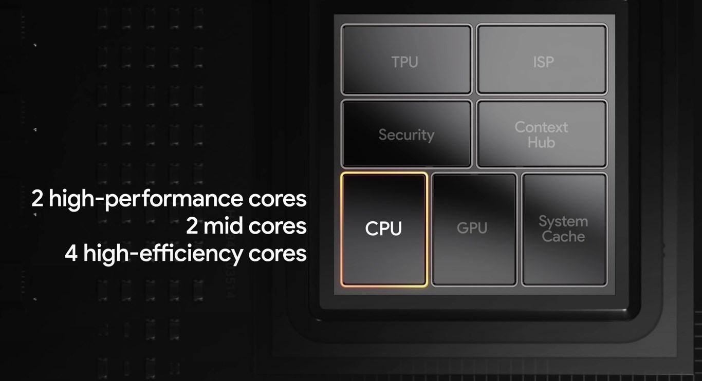
Google’s CPU setup is quite unusual from other SoCs in that it features a 2+2+4 configuration. While this isn’t truly exceptional – Samsung had this very same setup for the Exynos 9820 and Exynos 990 – the X1+A76+A55 configuration on the Tensor is currently unique in the market. Most other vendors and implementations out there have shifted over to a 1+3+4 big+mid+little CPU configurations.
On the Cortex-X1 side, Google’s use of a pair of cores means that, in theory, the performance of the chip with two heavy threads should be higher than any other Android SoC which only have a single big large performance core. The frequencies of the X1 pair come in at 2.8GHz, slightly lower than the 2.86GHz of the Snapdragon 888 and 2.91GHz of the Exynos 2100 X1 cores. Google equipped the cores with the full 1MB of L2 cache, similar to the S888 and double that of the E2100 configuration.
As for the middle cores, Google has employed Cortex-A76 cores, which has been a hot topic for discussion. At first glance, it’s seemingly a bit irrational considering both the Cortex-A77 and A78 offer higher performance and higher energy efficiency. The cores are clocked at 2.25GHz and come with 256KB of L2. We haven’t received a clear explanation from Google as to why they used the A76, but I do think it’s likely that at the time of design of the chip, Samsung didn’t have newer IP ready for integration. The chip has been brewing for some time and while it does feature X1 cores, maybe it was too late in the process to also shift over to newer middle cores. I do not think there was a purposeful choice of using A76 cores instead of A78, since as we’ll see in our performance benchmarks that the older design underperforms.
On the little cores, there are 4x A55 cores at 1.8GHz. In contrast to Samsung’s own Exynos chips, Google has decided to equip the cores with 128KB of L2 caches rather than just 64KB, so they’re more in line with the Snapdragon 888 configuration. One odder choice from Google is that the L3 cache of the cluster is on the same clock plane as the A55 cores, which has latency and power implications. It’s also at odds with the dedicated L3 clock plane we see on the Exynos 2100.
Another Fat Mali GPU: G78MP20 At High Clocks
Earlier rumors about the SoC indicated that it would come with a Mali-G78 generation GPU, however we didn’t know the exact core count or clocks of the design. Google has since confirmed the MP20 configuration, which is the second-largest Mali GPU configuration, behind only the Kirin 9000 and its massive 24-core unit. I had initially theorized that Google was likely running the GPU at low frequencies to be able to optimize for energy efficiency, only to end up rather shocked to see that they’re still running the GPU at a peak clockspeed of 848MHz for the shader cores, and 996MHz for the tiler and L2. The Google Tensor, if I’m not mistaken, seems to be the first confirmed G78 implementation actually taking advantage of Arm’s split clock plane design of the G78, which allows the shared GPU fabric to run at a higher frequency than the actual shader cores – and hence why it has two frequencies.
The actual frequencies are extremely high. The Exynos 2100’s G78MP14 already ran at 854MHz, and it was a chip which we deemed to have very high peak power figures; but here Google is adding 42% more cores and is not backing down on frequency. So that’s very eye-brow raising and concerning in terms of peak GPU power, concerns which we’ll see materialize in the latter GPU evaluation section.
LPDDR5, 8MB SLC Cache
The memory controllers on the Google Tensor appear to be the same as on the Exynos 2100, supporting LPDDR5 in a 4x 16-bit channel configuration for a total peak theoretical bandwidth of 51.2GB/s.
Google also integrated 8MB of system cache, and for me it isn’t exactly clear if this is the same IP Samsung uses on the Exynos 2100. Seemingly they’re both 8MB, but I’m leaning towards saying that it’s a different IP, or at the very least a different version of the IP, as there are some real differences in the way it’s architected and how it behaves.
Google here makes very extensive usage of the SLC for improving the performance of the SoC blocks, including their own custom blocks. The SLC allows itself to be partitioned and to dedicate SRAM regions to particular IP blocks on the SoC, giving them exclusive access to all or parts of the cache in varying use-case situations.
A Custom Hybrid ISP Pipeline
Usually when people or companies talk about SoC ISPs, these are always depicted as being a single monolithic IP block. In reality what we call an “ISP” is a combination of different specialized IP blocks, each handling different tasks in what we call the imaging pipeline. The Google Tensor here is interesting in that it takes bits and pieces of what Samsung uses on their Exynos chips, and also integrates custom Google-developed blocks into the pipeline – something Google actually talked about in their presentation of the SoC.
The imaging system uses IP blocks that correspond to an Exynos imaging pipeline, such as pixel phase detection processing units, contrast autofocus processing units, image scalers, distortion correction processing blocks and view-dependent occlusion texture function processing blocks. What’s lacking here is that some other processing blocks are missing, which I imagine are related to more post-processing computation blocks that Samsung uses.
The Google developed IP blocks in the ISP chain seem to be their own 3AA IP (Auto-Exposure, Auto-White Balance, Auto-Focus), as well as a custom pair of temporal noise-reduction IP blocks that are able to align and merge images. These are likely the custom blocks that Google was talking about when saying that they’ve developed blocks which help accelerate the kind of image processing that they employ as part of the Pixel lineup’s computational photography, and inarguably represent very important parts of the image processing pipeline.
Google's edgeTPU - What Makes the Tensor a Tensor
By now, it’s been quite clear that the big central talking point of the Google Tensor has been its TPU – or its Tensor Processing Unit. The TPU is, as its name implies, a custom Google developed-IP block that the company has been working on for a few years now. Until now, Google just called it the TPU inside the Tensor SoC, but at the driver level the company calls the block their “edgeTPU”. This is quite interesting as signals that the block is related to the ASIC “Edge TPU” that Google had announced back in 2018. The discrete chip had been advertised at 4 TOPs of processing power in 2 Watts of power, and while Google doesn’t advertise any performance metrics on the TPU inside the Tensor, there are entries showcasing the block goes up to 5W of power. So if the two are indeed related, then given the significant process node advantages and overall much newer IP, the performance figures of the Tensor TPU (sic) should be extremely significant.
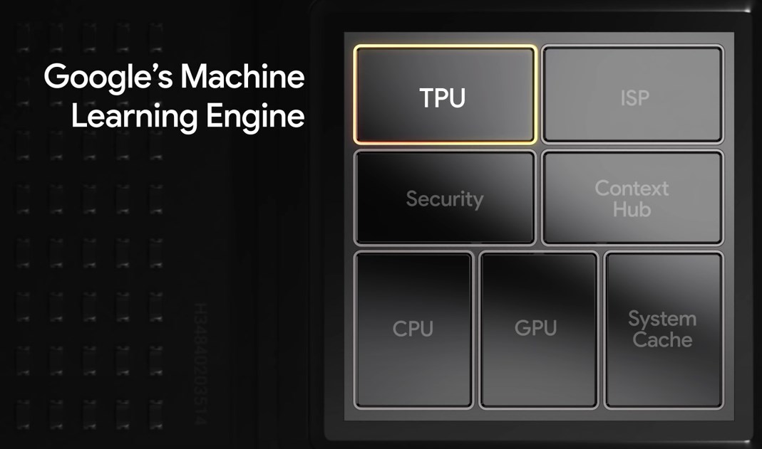
The block is very much the pride of Google’s silicon team, telling us that it’s using the latest architecture for ML processing that’s been optimized for the way Google’s R&D teams run machine learning within the company, and promises to allow for opening up the kind of new and unique use-cases that were the main goal for making a custom SoC in the first place. We’ll go into the product-side use-cases in a more Pixel focused review later on, but the performance metrics of the TPU do appear to be impressive.
The TPU block also seems to come with some sort of block that Google calls “GSA”. This is just speculation on my part here based on the drivers, but this seems to be some sort of control block that is in charge of operating the TPU firmware, and I think contains a quad-core Cortex-A32 CPU setup.
Media Encoders, Other Stuff
On the media encoder side, the Tensor SoC uses both Samsung’s own Multi-Function Codec IP block (which is identical to what’s used on the Exynos series) as well as what appears to be a Google IP block that is dedicated to AV1 decoding. Now this is a bit weird, as Samsung does advertise the Exynos 2100 as having AV1 decode abilities, and that functionality does seem to be there in the kernel drivers. However on the Galaxy S21 series this functionality was never implemented on the Android framework level. I have no good explanation here as to why – maybe the IP isn’t working correctly with AV1.
The Google IP block, which the company calls “BigOcean”, is a dedicated AV1 decoder, and this does actually expose AV1 decoding ability to the Android framework. The very weird thing here is that all it does is AV1 – every other encoding and decoding of other formats is left over to the Samsung MFC. It’s an interesting situation and I’m left to wonder where things evolve in the next-gen SoC.
Other differences for the Tensor SoC are for example the audio subsystem. Samsung’s SoC low-power audio decoding subsystem is thrown out in favor of Google’s own block design, I didn’t dwell too much into it but generally both blocks have the same task of allowing low-power audio playback without needing to wake up large parts of the SoC. I think this block (or the GSA) is also responsible as the always-on context-hub for sensor data aggregation, with the Tensor here using Google’s IP and way of doing things versus the Exynos variant of the same block.
Google also employs a fixed function hardware memory compressor in the form of a block called Emerald Hill, which provides LZ77 compression acceleration for memory pages, and can in turn be used to accelerate ZRAM offloading in swap. I’m not sure if the Pixels are currently running this out of the box, but should be able to be confirmed by seeing “lz77eh” in /sys/block/zram0/comp_algorithm , if somebody is able to read that out. As an anecdote, as far back as 5 years ago Samsung integrated similar hardware compression IP blocks into their SoCs for the very same task, but for some reason those were never enabled for shipping devices. Maybe the energy efficiency didn’t pan out as they thought it would.
External Exynos Modem - First non-Qualcomm mmWave Phones?
Since it’s a phone SoC, naturally the Tensor needs some sort of cellular connectivity. This is another area where Google is relying on Samsung, using the company’s Exynos Modem 5123. But, unlike the Exynos 2100 and its integrated modem, the Tensor uses a discrete external variant. As to why it’s discrete, it’s likely that with the massive GPU, larger CPU setup (two X1’s with full 1MB L2’s), and unknown size of the TPU, that the Tensor chip is quite large even in relation to the Exynos 2100.
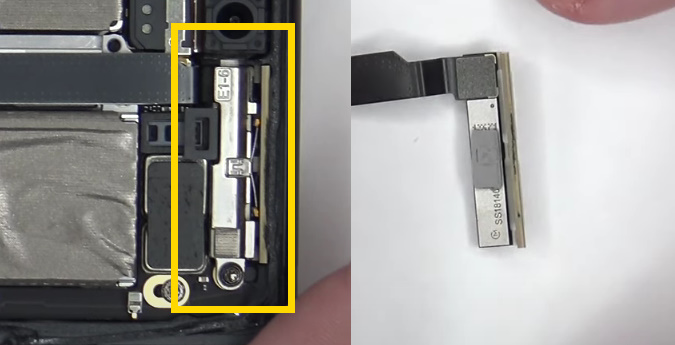
Source: PBKreviews
Another theory on my side is that Google would somehow still be tied to Qualcomm for US networks – either for CDMA or mmWave 5G connectivity. Surprisingly, it seems this isn’t the case, as the Pixel 6 series ships with the Exynos modem across the globe. That makes the Pixel 6 family particularly interesting, as it seems that this is the first non-Qualcomm mmWave implementation out there. For reference, Samsung had talked about their mmWave RFICs and antenna modules back in 2019, saying there were plans for 2020 devices. Whether that meant designs starting in 2020 (which the Pixel 6 series would be) or commercial availability wasn’t clear at the time, but it seems that these are the first commercial phones with the solution. I don’t expect to have mmWave coverage here for myself for another few years, but third-party reports showcase the phone reaching up to 3200Mbps while other field-tests showing around half of the practical speeds of Qualcomm devices. I hope more people in the next weeks and months will have the opportunity to dive deeper into the modem’s performance characteristics.
Semi-Custom Seems Apt
Overall, the Google Tensor ends up being almost exactly what we expected the chip to be, from the earliest reports of a collaboration between Google and Samsung. Is it a Google chip? Yes, they designed it in the sense that they defined it, while also creating quite a few Google-unique blocks that are integral to the chip's differentiation. Is it a Samsung Exynos chip? Also yes, from a more foundational SoC architecture level, the Tensor has a great deal in common with Samsung’s Exynos designs. In several areas of the Tensor there are architectural and behavioral elements that are unique to Samsung designs, and aren’t found anywhere else. To that end, calling the Google Tensor a semi-custom design seems perfectly apt for what it is. That being, said, let’s see how the Tensor behaves – and where it lands in terms of performance and efficiency.


108 Comments
View All Comments
sharath.naik - Thursday, November 4, 2021 - link
Good in-depth review. I know you are doing the camera review of this. So I have a request can you look into if the Pixel 6 cameras are hardware binned to ~12MP even though the specs say they are 50MP/48MP. There is a lot of mixed views out there, most mistaking this as the pixel binning done on other phones like galaxy S21u(Software binned for low light but has access to full resolution). If you could confirm this for the review would be great, looking forward to that review.Silver5urfer - Tuesday, November 2, 2021 - link
Exactly as expected 1:1The SoC is a bust, they tried to do some gimmickry with their zero talent and tried to make it a cheaper deal by going to Samsung for their IP fabrication expertise and lithography process. Ended up being a dud in CPU, GPU and price to performance, all that NPU NN, mega magic boom is all a farce. I was asking the same thing, what does these provide to us end users ? Nothing. Just that fancy Livetranslation and other gimmicks which you use seldom. On top we do not even know what TPU does in the Pixel Software, it's closed source. AOSP is open but Pixel UI and all backend are closed.
Hardware is utter joke, the P6 series has garbage mmwave system look at the internals, they crammed one lol. LG V50 back in 2019 had 2-33 mmwave antennas. This junk saved on cost. The display has banding issues all over the place. Optical image sensor for Fingerprint is slow and a joke vs the physical dedicated ones. The stereo speaker system has massive channel imbalance on top. Then you have the low battery SoT for this price point and battery capacity. The DIY aspect is thrown into gutters, the phone has massively hamfisted cooling approach with graphite pads smeared all over the place as leaks showed and no proper HS system it's just a small pathetic AL board reinforcement plate doing it so on top the Display has no metal backplate to reinforce it or dissipate heat. What a nonsense. SD888 itself heats up a lot and so many vendors add VC cooling, Sony Xperia 1 Mark 3 messed up there and had inferior performance with throttling. This junk is even more pathetic, pay for a S tier SKU get trash sustained performance of a B+ device, the AP, Pocket now and other Youtube shill press will hype this to moon.
We do not even know how this junk has in terms of Software blocks like P2, P3, P4 had A/B system, then merged partitions, later read only ext4 system. This will have even worse. To make it a round about trash, the software is a joke cheap kiddo inspired garbage, heck that BBKs OnePlus's Oxygen + Oppo Color OS mix is way superior than this junk with massive information density loss.
I'd wait for the next SD successor device, hopefully 888's BS power consumption and insane heat can be reduced.
Silver5urfer - Tuesday, November 2, 2021 - link
It's a typo for mmwave, it's 2-3 units. Also I forgot to mention the lack of charger, SD slot, no 3.5mm jack very poor servicing almost impossible to get the phone properly cooled if you open it due to cheap graphite pad reliance. It also has that USB port and microphone soldered to the mainboard which looks like a feeble trash unit check any phone in the recent times and look how solid engineered they are, dual sandwich designs with reinforced chassis and proper heat dissipation.goatfajitas - Tuesday, November 2, 2021 - link
People get WAY too hung up on benchmarks. LOL, a "dud". A phone is about user experience, not how many "geekmarks" = best.lionking80 - Tuesday, November 2, 2021 - link
I agree that the benchmarks do not tell the whole story, but I would still say that even the use of a Snapdragon 870 would have been a better choice.The general performance is similar (maybe a small advantage for Tensor in AI), but the advantages of Snapdragon 870 are bigger: runs much cooler, hugely better battery-life.
To be honest I am disappointed by the SOC. The only thing that might make it a seller is the software (ui and camera), but the SOC is rather a no-go.
goatfajitas - Tuesday, November 2, 2021 - link
There are other factors though. Early ROM settings, tweaks, bugs, and cooling/hardware. The 870 may have scored lower in a P6 as well. So many factors. - Agreed, the P6 should be a bit more polished though.at_clucks - Tuesday, November 2, 2021 - link
The problem goes beyond the slightly worse SoC than the already existing Qualcomm offering. It's that despite being a "Google SoC" they still support it for just 3 years. All the excuses used over the years, all the pointing fingers at SoC manufacturers for the lack of support were just proven to be a load of crap. Same crap, now with a google sticker.sharath.naik - Tuesday, November 2, 2021 - link
It's about to get worse with the camera review. I can verify Google might have been bluffing about the 50mp/48mp sensors. The sensors are locked at 12mp. So Pixel pro has essentially three 12 mp cameras. Which means the portrait mode zoom of 2x is a low resolution 3 MP image. Also at 10x zoom the image resolution is 2.5MP, 4 times lower than that of s21 ultra. What drove Google to make the choice of first hardware pixel binning the resolution down and then trying to digitally blow the resolution backup!!.It's baffling, tried to get an answer from Google support, they just refused to confirm or deny this is binned at the hardware levelhoxha_red - Tuesday, November 2, 2021 - link
"I can verify that google might have been bluffing"dude, lmfao—it's called "binning"; please look it up. they've been upfront about this and it was known before the phone was even launched, let alone after we've seen all of these reviews. The reason Google support "refused to confirm or deny" is because the people doing customer support are unlikely to know what "pixel binning" is (hey, I guess they're in good company there with you), and are not equipped to deal with weirdos of your specific variety.
Maxpower27 - Tuesday, November 2, 2021 - link
You obviously have no familiarity with mobile phone cameras and sensors in particular. Read up about them and then try again.