SK Hynix: HBM2E Memory Now in Mass Production
by Ryan Smith on July 2, 2020 10:00 AM EST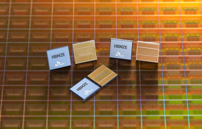
Just shy of a year ago, SK Hynix threw their hat into the ring, as it were, by becoming the second company to announce memory based on the HBM2E standard. Now the company has announced that their improved high-speed, high density memory has gone into mass production, offering transfer rates up to 3.6 Gbps/pin, and capacities of up to 16GB per stack.
As a quick refresher, HBM2E is a small update to the HBM2 standard to improve its performance, serving as a mid-generational kicker of sorts to allow for higher clockspeeds, higher densities (up to 24GB with 12 layers), and the underlying changes that are required to make those happen. Samsung was the first memory vendor to ship HBM2E with their 16GB/stack Flashbolt memory, which runs at up to 3.2 Gbps in-spec (or 4.2 Gbps out-of-spec). This in turn has led to Samsung becoming the principal memory partner for NVIDIA’s recently-launched A100 accelerator, which was launched using Samsung’s Flashbolt memory.
Today’s announcement by SK Hynix means that the rest of the HBM2E ecosystem is taking shape, and that chipmakers will soon have access to a second supplier for the speedy memory. As per SK Hynix’s initial announcement last year, their new HBM2E memory comes in 8-Hi, 16GB stacks, which is twice the capacity of their earlier HBM2 memory. Meanwhile, the memory is able to clock at up to 3.6 Gbps/pin, which is actually faster than the “just” 3.2 Gbps/pin that the official HBM2E spec tops out at. So like Samsung’s Flashbolt memory, it would seem that the 3.6 Gbps data rate is essentially an optional out-of-spec mode for chipmakers who have HBM2E memory controllers that can keep up with the memory.
At those top speeds, this gives a single 1024-pin stack a total of 460GB/sec of memory bandwidth, which rivals (or exceeds) most video cards today. And for more advanced devices which employ multiple stacks (e.g. server GPUs), this means a 6-stack configuration could reach as high as 2.76TB/sec of memory bandwidth, a massive amount by any measure.
Finally, for the moment SK Hynix isn’t announcing any customers, but the company expects the new memory to be used on “next-generation AI (Artificial Intelligence) systems including Deep Learning Accelerator and High-Performance Computing.” An eventual second-source for NVIDIA’s A100 would be among the most immediate use cases for the new memory, though NVIDIA is far from the only vendor to use HBM2. If anything, SK Hynix is typically very close to AMD, who is due to launch some new server GPUs over the next year for use in supercomputers and other HPC systems. So one way or another, the era of HBM2E is quickly ramping up, as more and more high-end processors are set to be introduced using the faster memory.
Source: SK Hynix


37 Comments
View All Comments
Strunf - Monday, July 6, 2020 - link
Right let's stack one bad thermal conductor on top of a power hungry device, makes sense...nVIDIA will never die on the dGPU, their dGPU is today an extension of their other business and creating a dGPU costs them little since it's shares most of their technology with other products.
Anyways Intel would kill AMD faster than AMD would kill NVIDIA, NVIDIA owns the GPU high end and nothing seems to stop them, if Intel comes up with a decent iGPU it will eat AMD market share on the low end and AMD will be left with little to nothing.
Ej24 - Thursday, July 2, 2020 - link
their GCN architecture required huge memory bandwidth to be efficient and reach high performance. To reach this speed with GDDR5 would have required 512bit bus which would consume like 75W of power for the memory alone. HBM could provide more bandwidth with only like ~15W of power. It was out of necessity to make the gcn architecture perform competitively while staying within a reasonable power limit.Quantumz0d - Friday, July 3, 2020 - link
THIS. So many miss this aspect of GCN-HBM relation.Jorgp2 - Thursday, July 2, 2020 - link
Fuck that.HBM is amazing for water-cooling, and small form factor GPUs
zodiacfml - Saturday, July 4, 2020 - link
One of AMD's strategy to compete with Nvidia is to use better memory hardware across their products, back then. Nvidia should be using HBM on consumer gaming cards to improve volumes and make HBM standard, at least on high end.I like the Sapphire Vega 56 design so much that I bought it wihle it is expensive during the cryptomining craze. Too bad for me that I game so little.
Deicidium369 - Sunday, July 5, 2020 - link
Nvidia is the biggest user of HBM - it is standard on their high end - their high end is compute cardsDribble - Monday, July 6, 2020 - link
It was more of a strategy to allow them to continue to use an inefficient gpu design - Vega/Polaris were way behind Nvidia on efficient usage of memory bandwidth. AMD couldn't afford to fix this so they sticking plastered over it by attaching very fast HBM memory which made their cards expensive and harder to make but was the only way they could stay competitive.quorm - Thursday, July 2, 2020 - link
Hoping for more apus with integrated hbm.quorm - Thursday, July 2, 2020 - link
Maybe when AMD gets around to putting RDNA in their apus they can glue in some hbm, too.jeremyshaw - Thursday, July 2, 2020 - link
It's AMD. I'd venture AMD will wait until after Intel starts offering Intel "APUs" with HBM2E (or later), before even considering it for their own AMD laptop APUs.