AMD Clarifies Comments on 7nm / 7nm+ for Future Products: EUV Not Specified
by Dr. Ian Cutress on March 5, 2020 6:50 PM EST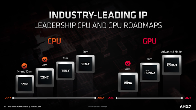
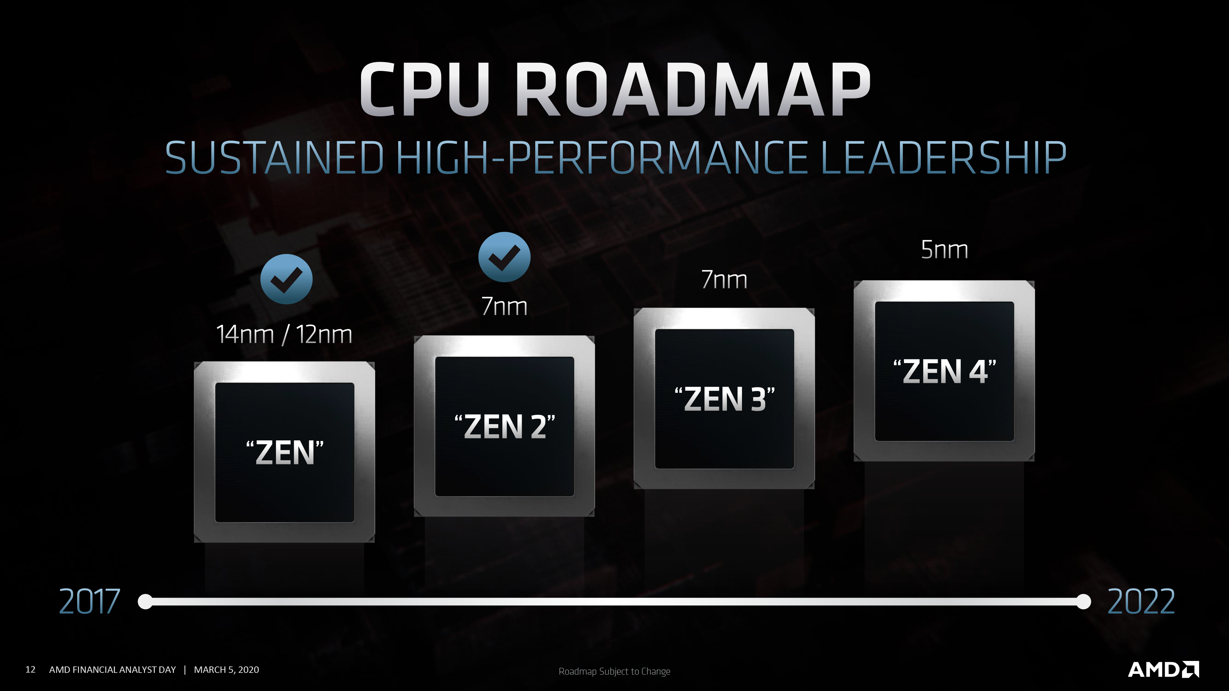
As part of AMD’s Financial Analyst Day 2020, the company gave the latest updates for its CPU and GPU roadmap. A lot of this we have seen before, with the company talking out to Zen 4 and Genoa on its datacenter CPU product line, out to Zen 3 and Ryzen 4000 with the consumer product line, and now with the RDNA/CDNA split between consumer and compute graphics. In previous graphs of a similar nature, AMD used the term ‘7nm+’ when referring to products beyond the first iteration of 7nm. AMD has today clarified to us that this does not mean they are using TSMC’s N7+ process node for those items.
TSMC has three high-level versions of its 7nm process:
- N7, which is the basic initial version using ‘DUV’ only tools (so no EUV),
- N7P, which is the second generation version of N7 which is also only DUV
- N7+, which is an EUV version of N7 for a number of layers in the metal stack
This nomenclature has been finalized within the past year or so.
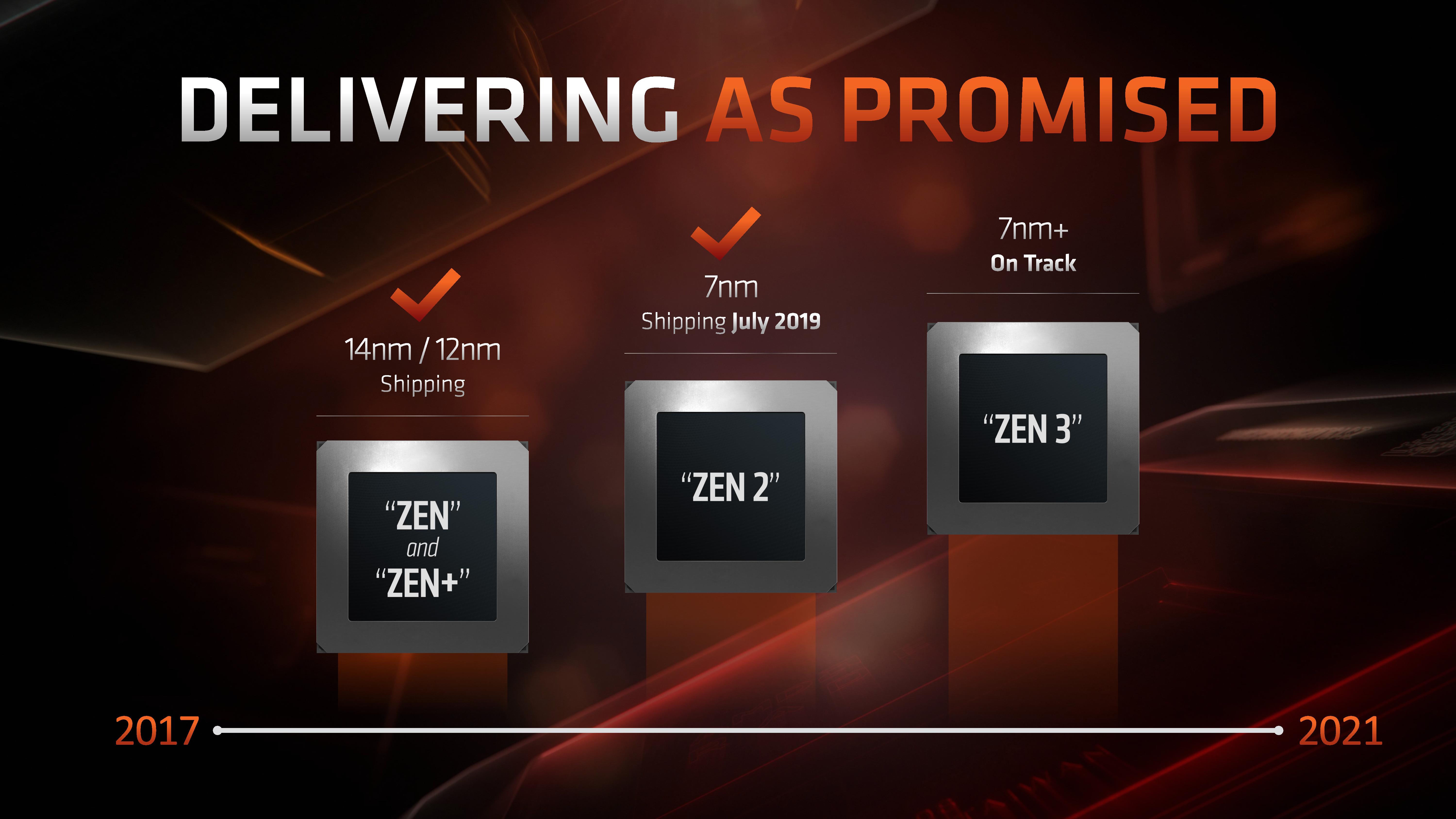
Before this, AMD had presented various CPU and GPU roadmaps to the public. For the Zen 2 hardware, such as Ryzen 3000 series (Matisse), AMD had labeled this as ‘7nm’, which was all widely interpreted to mean TSMC’s N7 process. For future products, such as Zen 3, AMD had the slide listed as ‘7nm+’, which everyone had understood was ‘a better version of 7nm’.

Example Roadmap from CES 2018
From Next Horizons in July 2019
Because AMD labeled those as 7nm+, when TSMC called its version of 7nm with EUV to be N7+, one of the obvious assumptions that people have made is that where AMD wrote 7nm+, it was to be on the N7+ process. We have since learned that this is not entirely correct.
In order to avoid confusion, AMD is dropping the ‘+’ from its roadmaps. In speaking with AMD, the company confirmed that its next generations of 7nm products are likely to use process enhancements and the best high-performance libraries for the target market, however it is not explicity stating whether this would be N7P or N7+, just that it will be ‘better’ than the base N7 used in its first 7nm line.
This doesn’t necessarily mean that AMD isn’t going to be using EUV in the future – we were told it will be on a case by case basis, and at this time they wanted to clarify that AMD is not making any specific clarifications of which version of 7nm from TSMC it plans to use. More will be detailed at future events.
Interested in more of our AMD Financial Analyst Day 2020 Coverage? Click here.


37 Comments
View All Comments
ksec - Friday, March 6, 2020 - link
I find this sentiment very strange, I will have to dig up old information to prove my point, but working on top of my headAMD clearly stats 7nm+ means 7nm EUV. That was written on their roadmap somewhere. It wasn't the confusion of N7+ or N7P. I think this is a spin that tries to control expectation.
I think it is likely AMD at least intend to use 7nm EUV for Zen 3 at first, but their just isn't enough capacity AMD would like, and sticking to a more mature N7P and later N6 would be a far better option.
dotjaz - Friday, March 6, 2020 - link
Where did they "clearly stats" 7nm+ means 7nm EUV and even if that were the case, why would that be N7+? AMD never used N7, they used N7 "Large Die", with 1.45x M1/BEOL scaling instead of 1x and so on, very different from the baseline N7.Why would AMD transition to an IP incompatible version (N7+ based) when by then, the IP compatible version of 7nm, N6 would be available?
scineram - Thursday, March 12, 2020 - link
Because it is not.eastcoast_pete - Saturday, March 7, 2020 - link
Why does it even matter if AMD's chiplets are made using EUV, some EUV, or DUV, unless that makes a significant difference in power consumption or thermals thus justifying the costs? EUV is definitely here (ASML sold enough EUV scanners to validate that), but the yield is still way below DUV. Thus, it makes sense to Fab chips where power consumption is critical (smartphone SoCs etc) all or in part with EUV, and desktop CPUs and GPUs with the best compromise between cost (yield) and power consumption.Regarding desktop and laptop AMD CPUs and APUs, I expect the biggest improvements in power consumption to come from more efficient interconnects.
JKflipflop98 - Sunday, March 8, 2020 - link
It would be almost impossible to fab a true 7nm part without EUV. You'd need octuple patterning at the contacts. This just goes to show how far from 7nm they really are. Their 7nm is more like 16 or so.scineram - Thursday, March 12, 2020 - link
No.ankitadave - Wednesday, August 26, 2020 - link
I recorded this article, a resolution of gratefulness is all Mumbai accompanies all things considered for sharing this content. This is inconceivably supporting for one and all and marvelous.http://www.mumbaiescortshub.in/