Early TSMC 5nm Test Chip Yields 80%, HVM Coming in H1 2020
by Dr. Ian Cutress on December 11, 2019 7:05 PM EST
Today at the IEEE IEDM Conference, TSMC is presenting a paper giving an overview of the initial results it has achieved on its 5nm process. This process is going to be the next step for any customer currently on the N7 or N7P processes as it shares a number design rules between the two. The new N5 process is set to offer a full node increase over the 7nm variants, and uses EUV technology extensively over 10+ layers, reducing the total steps in production over 7nm. The new 5nm process also implements TSMC’s next generation (5th gen) of FinFET technology.
The Headline Numbers
If you’re only here to read the key numbers, then here they are. In the disclosure, TSMC is stating that their 5nm EUV process affords an overall with a ~1.84x logic density increase, a 15% power gain, or a 30% power reduction. The current test chip, with 256 Mb of SRAM and some logic, is yielding 80% on average and 90%+ in peak, although scaled back to the size of a modern mobile chip, the yield is a lot lower. The technology is currently in risk production, with high volume production scheduled for the first half of 2020. This means that chips built on 5nm should be ready in the latter half of 2020.
From WikiChip
TSMC's 7nm process currently yields just shy of 100 million transistors per square millimeter (mTr/mm2) when using dense libraries, about 96.27 mTr/mm2. This means that the new 5nm process should be around 177.14 mTr/mm2.
The Details on Yield
As part of any risk production, a foundry produces a number of test chips in order to verify that the process is working expected. For 5nm, TSMC is disclosing two such chips: one built on SRAM, and other combing SRAM, logic, and IO.
For the SRAM chip, TSMC is demonstrating that it has both high current (HC) and high density (HD) SRAM cells, at a size of 25000 nm2 and 21000 nm2 respectively. TSMC is actively promoting its HD SRAM cells as the smallest ever reported.
For the combined chip, TSMC is stating that the chip consists of 30% SRAM, 60% Logic (CPU/GPU), and 10% IO. In that chip are 256 mega-bits of SRAM, which means we can calculate a size. A 256 Mbit SRAM cell, at 21000 nm2, gives a die area of 5.376 mm2. TSMC states that this chip does not include self-repair circuitry, which means we don’t need to add extra transistors to enable that. If the SRAM is 30% of the chip, then the whole chip should be around 17.92 mm2.
For this chip, TSMC has published an average yield of ~80%, with a peak yield per wafer of >90%. Knowing the yield and the die size, we can go to a common online wafer-per-die calculator to extrapolate the defect rate. To make things simple, we assume the chip is square, we can adjust the defect rate in order to equal a yield of 80%. Using the calculator, a 300 mm wafer with a 17.92 mm2 die would produce 3252 dies per wafer. An 80% yield would mean 2602 good dies per wafer, and this corresponds to a defect rate of 1.271 per sq cm.

So, a 17.92 mm2 die isn’t particularly indicative of a modern chip on a high performance process. The first chips on a new process are often mobile processors, especially high-performance mobile processors that can amortize the high cost of moving into a new process. These chips have been increasing in size in recent years, depending on the modem support. For example, the Kirin 990 5G built on 7nm EUV is over 100 mm2, closer to 110 mm2. One could point to AMD’s Zen 2 chiplet as more applicable chip, given it comes from a non-EUV process which is more amenable to moving to 5nm EUV, however something like this will come later and will use high performance libraries to not be as dense.
In that case, let us take the 100 mm2 die as an example of the first mobile processors coming out of TSMC’s process. Again, taking the die as square, a defect rate of 1.271 per cm2 would afford a yield of 32.0%. This is pretty good for a process in the middle of risk production. A yield rate of 32.0% for a 100 mm2 chip would even be sufficient for some early adopters wanting to get ahead of the game.
(For anyone wanting to compare this defect density to the size of Zen 2 chiplet at 10.35x7.37mm, that equates to 41.0% yield.)
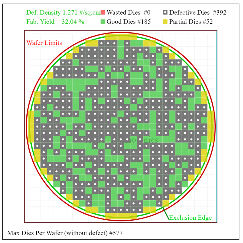
(Note initially when I read it the first time, I saw this only in the context of the 5.376 mm2 SRAM-only die. Doing the math, that would have afforded a defect rate of 4.26, or a 100mm2 yield of 5.40%. This is very low. The paper is a little ambiguous as to which test chip the yields are referring to, hence my initial concern at only a 5.4% yield. In conversing with David Schor from Wikichip, he says that even the 32.0% yield for 100 mm2 calculated is a little low for risk production, unless you’re happy taking a lot of risk.)
TSMC’s Test Chip: CPU and GPU Frequency
Of course, a test chip yielding could mean anything. A successful chip could just ‘turn on’, and the defect rate doesn’t take into account how well the process can drive power and frequency. As part of the disclosure, TSMC also gave some ‘shmoo’ plots of voltage against frequency for their example test chip.
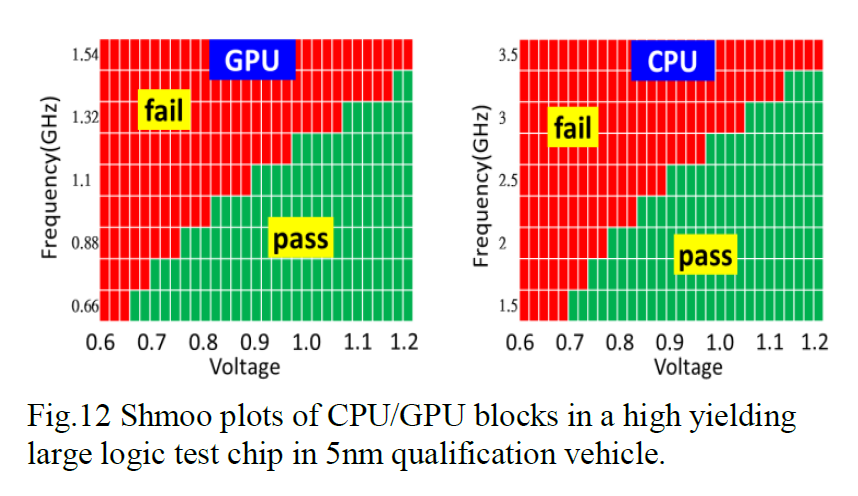
For CPU, the plot shows a frequency of 1.5 GHz at 0.7 volts, all the way up to 3.25 GHz at 1.2 volts.
For GPU, the plot shows a frequency of 0.66 GHz at 0.65 volts, all the way up to 1.43 GHz at 1.2 volts.
One could argue that these aren’t particularly useful: the designs of CPUs and GPUs are very different and a deeply integrated GPU could get a much lower frequency at the same voltage based on its design. Unfortunately TSMC doesn’t disclose what they use as an example CPU/GPU, although the CPU part is usually expected to be an Arm core (although it might only be a single core on a chip this size). It often depends on who the lead partner is for the process node.
IO Demonstration: PAM4
One of the key elements in future chips is the ability to support multiple communication technologies, and in the test chip TSMC also included a transceiver designed to enable high-speed PAM-4.

We have already seen 112 Gb/s transceivers on other processes, and TSMC was able to do 112 Gb/s here with a 0.76 pJ/bit energy efficiency. Pushing the bandwidth further, TSMC was able to get 130 Gb/s still within tolerances in the eye diagram, but at a 0.96 pJ/bit efficiency. This bodes well for any PAM-4 based technologies, such as PCIe 6.0.
Using EUV: A Reduction in Mask Count
Having spent a number of processes built upon 193nm-based ArF immersion lithography, the mask count for these more and more complex processors has been ballooning. What used to be 30-40 masks on 28 nm is now going above 70 masks on 14nm/10nm, with reports that some leading edge process technologies are already above 100 masks. With this paper, TSMC is saying that extensive use of EUV for over 10 layers of the design will actually, for the first time, reduce the number of process masks with a new process node.
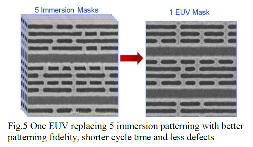
The benefit of EUV is the ability to replace four or five standard non-EUV masking steps with one EUV step. This comes down to the greater definition provided at the silicon level by the EUV technology. The flip side is that the throughput of a single EUV machine (175 wafers per hour per mask) is much slower than a non-EUV machine (300 wafers per hour per mask), however the EUV’s speed should be multiplied by 4-5 to get a comparison throughput. TSMC’s extensive use, one should argue, would reduce the mask count significantly. Ultimately it’s only a small drop.
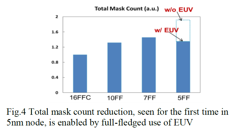
If we assume around 60 masks for the 16FFC process, the 10FF process is around 80-85 masks, and 7FF is more 90-95. With 5FF and EUV, that number goes back down to the 75-80 number, compared to the 110+ that it might have been without EUV. This simplifies things, assuming there are enough EUV machines to go around. Recent reports state that ASML is behind in shipping its 2019 orders, and plans to build another 25-27 in 2020 with demand for at least 50 machines.
Transistor Types at 5nm
Part of the IEDM paper describes seven different types of transistor for customers to use. We’ve already mentioned the new types, eVT at the high end and SVT-LL at the low end, however here are a range of options to be used depending on the leakage and performance required.
![]()
The three main types are uLVT, LVT and SVT, which all three have low leakage (LL) variants. Then eLVT sits on the top, with quite a big jump from uLVT to eLVT.
The Effect of Design-Technology Co-Optimization (DTCO)
One of the features becoming very apparent this year at IEDM is the use of DTCO. In a nutshell, DTCO is essentially one arm of process optimization that occurs as a result of chip design – i.e. it can be very easy to design a holistic chip and put it onto silicon, but in order to get the best performance/power/area, it needs to be optimized for the process node for the silicon in question. The effects of this co-optimization can be dramatic: the equivalent of another process node jump in PPA is not something to be sniffed at, and it also means that it takes time to implement.
One downside to DTCO is that when applied to a given process or design, it means that any first generation of a future process node is technically worse than the holistic best version of the previous generation, or at best, on parity, but a lot more expensive. So in order to better the previous process technology, at least one generation of DTCO has to be applied to the new node before it can even be made viable, making its roll-out take even longer.
This is a persistent artefact of the world we now live in. Intel, TSMC, and to a certain extent Samsung, have to apply some form of DTCO to every new process (and every process variant) for specific products. For TSMC at least, certain companies may benefit from exclusive rights to certain DTCO improvements, to help those companies get additional performance benefits. But the fact that DTCO is needed just to draw parity means that we’re getting a further elongation of process node announcements: if it doesn’t come with a form of DTCO, it’s not worth announcing as no-body will want it.
Thankfully in TSMC’s 5nm paper at IEDM, the topic of DTCO is directly addressed. The 5nm test chip has an element of DTCO applied, rather than brute-forcing the design rules, which has enabled scaling of the design rules for an overall 40% chip size reduction. So that overall test chip, at 17.92 mm2, would have been more like 25.1 mm2, with a yield of 73%, rather than 80%. It doesn’t sound like much, but in this case every little helps: with this element of DTCO, it enables TSMC to quote the 1.84x increase in density for 15+% speed increase/30% power reduction.
Unfortunately, we don't have the re-publishing rights for the full paper. For those that have access to IEDM papers, search for
36.7 5nm CMOS Production Technology Platform featuring full-fledged EUV, and High Mobility Channel FinFETs with Densest 0.021 µm2 SRAM Cells for Mobile SoC and High Performance Computing Applications, IEEE IEDM 2019
One obvious data point that TSMC hasn't disclosed is the exact details on its fin pitch sizes, or contacted poly pitch (cpp), which are often quoted when disclosing risk production of new process nodes. We're hoping TSMC publishes this data in due course.


64 Comments
View All Comments
Fataliity - Wednesday, December 11, 2019 - link
Man you tried really hard there. To skew in Intel's favor. Why are you defending their failure? They chose their goals and so did TSMC. TSMC succeeded, Intel didn't. And I forget but I think TSMC's revenue on 7nm was somewhere around 34% of Total Revenue, which isn't low volume. It is their highest revenue node, beating 28nm too. It's nothing to do with volume.Also TSMC has much closer relationship to ASML. They first created HVM EUV with ASML engineers in THEIR lab. In 2013 I think. So of course they have more experience with EUV and DUV ASML machines, they are basically co-developing the technology. They also own a majority of patents on techniques.
The main reason is die size. Obviously AMD knew when switching to 7nm that big chips would not be sustainable, and opted for an MCM approach due to yields and complexities of quad-patterning. Which happened to be a very smart business move because below 7nm the yields get worse, so the smaller dies which benefit from the node is the CPU cores so the chiplet architecture was in hindsight a godsend. Whereas the IO is also most prone to failure from defects, was kept on a larger node with almost perfect yields.
You don't get to just change the timetables to help Intel look better. They were too ambitious, and failed. No matter how you spin it. It was their fault. I'm sure their masks play a key role in the failure too. The masks are very very important on DUV quad patterning.
Fataliity - Wednesday, December 11, 2019 - link
And to add to that, TSMC's revenue is strictly from creating chips for other people. Intel enjoys 70%? gross margin? or around there, while their Revenue's are very close recently if i remember correctly So obviously TSMC is producing many more chips (maybe not all on the leading node) versus Intel.lightningz71 - Thursday, December 12, 2019 - link
To add additional information, Intel also decided that, with their 10nm node, they wanted to make a material change in their gate and substrate formulation, and that proved to be harder to work with than they predicted. Basically, Intel made a bet that EUV would be more delayed than it is, and tried a different approach that would buy them two nodes of shrinkage without requiring EUV based patterning and masking. That bet failed spectacularly. EUV was ready for volume production earlier than Intel expected (though, much later than early industry targets) AND they couldn't get 10nm to behave with their material choices to the level that volume production requires.Compounding problems for Intel further, they HEAVILY optimize each core/chip layout for the targeted process node. This means that if there is a problem with a node, EVERYTHING gets delayed, and that porting the design to an older node requires a LOT more work and takes MUCH longer than it otherwise would. It also balloons the die size on those older nodes. Newer designs usually include a LOT more transistors than older ones. On older nodes, those transistors are easily half again larger, so they either have to use much larger dies, which reduces wafer yield, or they have to use far fewer core counts, resulting lower tier products that command a lower price on the market, reducing revenue per die. Neither is a good choice and both result in reduced revenues.
thestryker - Wednesday, December 11, 2019 - link
One thing to note about ASML is that Intel wrote off the whole first generation or two of EUV because it wasn't powerful enough for their needs. That could very well bite them in the ass long term, but they clearly have/had a plan which led to that choice.As far as Intel is concerned it was 100% being overly ambitious and not predicting new architecture + node problems. I do agree this is on them, but with luck it has been a lesson they learn from.
AMD was forced to go dramatically new due to revenue which is the real reason we saw MCM designs. It has also not been without its problems, but it seems like the best approach to huge core counts (I consider that 16c+).
Teckk - Wednesday, December 11, 2019 - link
Has Intel published anything like this for their 10++ or 7nm?ksec - Thursday, December 12, 2019 - link
No, Intel does not Fab for others ( at least not any more ) and does not require or have interest to disclose any of these.Compared to TSMC being a Pure Play Foundry.
Yojimbo - Wednesday, December 11, 2019 - link
So their N7 to N5 is like a half node shrink as far as power and performance characteristics.Teckk - Thursday, December 12, 2019 - link
N5 is a full node. Also, it says 30% reduction in power among other thing, which is pretty significant. Yet to see numbers from Intel, if their next (or current 10nm HVM) node after 14.Yojimbo - Saturday, December 14, 2019 - link
I said "like a half node in terms of power and performance characteristics". It's 15 percent performance OR 30 percent power improvement. Over a full-node 2 year time frame that's pretty terrible. Going from 20 nm to 16 nm, TSMC claimed 50% performance or 60% power improvement. 10 is an intermediate node between 16 and 7 and from 16 to 10 they claim 15% performance or 35% power and from 10 to 7 they claim 20% performance or 40% power, both better than the 7 to 5 claim. 5 seems a lot more like an intermediate node, performance-wise, only the time period from 7 to 3 is stretching out to 4 years from the 3 years it took to go from 16 to 7. Because it's getting stretched out so much and 3 nm won't be ready, they are adding N5P to what in recent history would have been a short term node used mostly for SOCs.Fataliity - Wednesday, December 11, 2019 - link
When you talk about the "exclusive rights" for specific transistor, you reffering to something similar to what Nvidia has on 14nm with their exclusive finfets?