AMD Teases First Navi GPU Products: RX 5700 Series Launches in July, 25% Improved Perf-Per-Clock
by Ryan Smith on May 26, 2019 11:30 PM EST- Posted in
- GPUs
- AMD
- Radeon
- Navi
- 7nm
- PCIe 4.0
- Computex 2019
- RX 5700 Series
While the bulk of this morning’s AMD Computex keynote has been on AMD’s 3rd generation Ryzen CPUs and their underlying Zen 2 architecture, the company also took a moment to briefly touch upon its highly anticipated Navi GPU architecture and associated family of products. AMD didn’t go too deep here, but they have given us just enough to be tantalized ahead of a full reveal in the not too distant future. The first Navi cards will be the Radeon RX 5700 series, which are launching in July and on an architectural level will offer 25% better performance per clock per core and 50% better power efficiency than AMD’s current-generation Vega architecture. The products will also be AMD's first video cards using faster GDDR6 memory. Meanwhile AMD isn’t offering much in the way of concrete details on performance, but they are showing it off versus NVIDIA’s GeForce RTX 2070 in the AMD-favorable game Strange Brigade.
A Peek At the Navi GPU Architecture
Compared to today’s Ryzen information AMD is being a lot more modest – there’s no specific SKU information for a start – but they are offering us our first architectural details on Navi since we learned in 2016 that it would bring “next gen memory” support. First and foremost, AMD has been tinkering with their GPU architecture to improve both the effective IPC and memory bandwidth efficiency. In what the company is calling their Radeon DNA (RNDA) archtiecture – I should note that it’s not clear if this is a branding exercise to downplay the GCN family name or if it's a more heavily overhauled architecture – AMD has revealed that Navi’s compute units have been redesigned to improve their efficiency. AMD's press materials also note that, regardless of the above changes, the size hasn't changed: a single CU is still 64 stream processors.
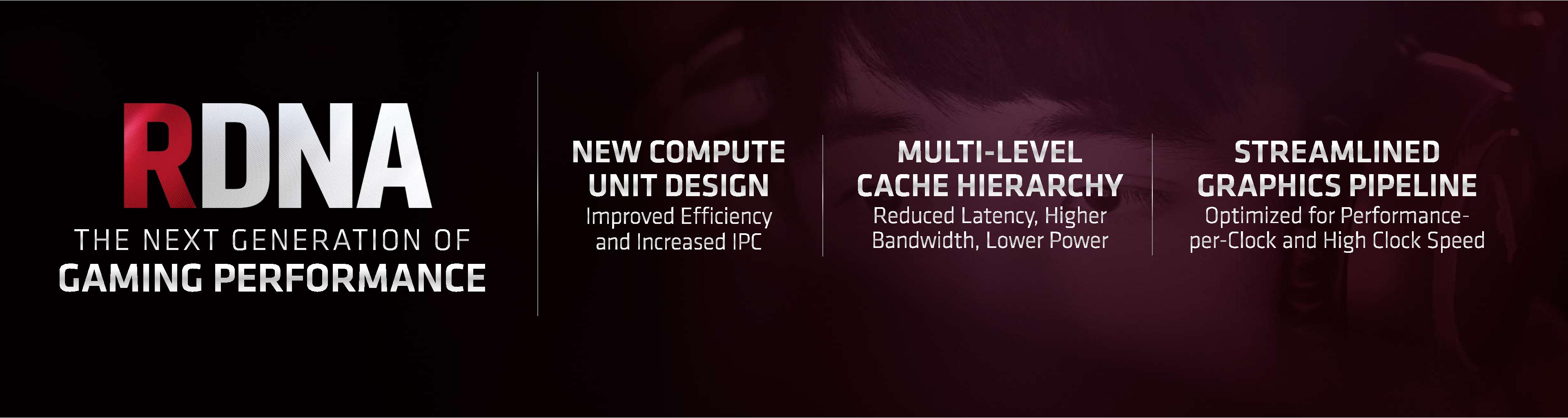
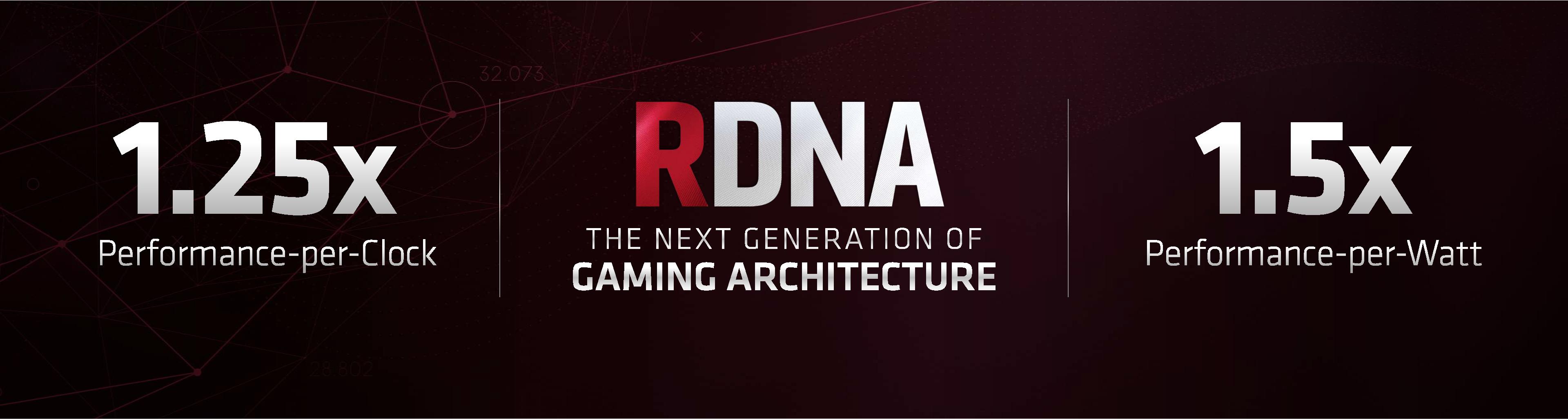
Altogether, a Navi core/CU should be 25% faster than a Vega core on a clock-for-clock basis. The devil is in the details of course – AMD's data is based off of their internal testing, taking the geomean of 30 games tested at 3840x2160 with Ultra settings and 4x AA, so it's not a holistic view of just the core architecture – but it’s still potentially one of AMD’s largest GPU IPC gains in the last several years. AMD’s presentation also noted that this was part of a larger streamlining of the graphics pipeline, which is designed for both higher IPCs and high clockspeeds. For reference, on the same process AMD has been able to push Radeon VII well past its comfort/efficiency point to 1750MHz, so it will be interesting to see how Navi compares.
Feeding the beast is a new multi-level cache hierarchy. AMD is touting that Navi’s cache subsystem offers both higher performance and lower latency than Vega’s, all for less power consumption. AMD has always been hamstrung a bit by memory/cache bottlenecks, so this would be a promising development for AMD’s GPU architecture. Meanwhile for a bit of reference, Vega already implemented a more modern cache hierarchy, so it would seem unlikely that AMD is changing their cache levels or what blocks are clients of which caches.
AMD's memory controllers themselves have also been updated. Long expected, and confirmed in the press release that went out after Dr. Lisa Su's keynote, the upcoming RX 5700 series cards use GDDR6 memory, which should give AMD's cards a hearty bandwidth bump over their comparable GDDR5 Polaris cards.
It's also worth noting that, fittingly, the new Navi parts support PCI Express 4.0 as well. This will actually be AMD's second GPU with PCIe 4.0 functionality – Vega 20 was first, but it's only enabled in the Radeon Instinct parts – so this is the first time it's enabled in a consumer part. Of course to make full use of it you'll need a PCI 4.0-capable host, which AMD is happy to sell you as well. As for the performance impacts, these remain to be seen. Thus far high-end AMD/NVIDIA parts haven't been significantly bottlenecked in games by PCIe 3.0 x16 (or even x8), so it will be interesting to see how much the extra bus bandwidth helps these first generation of parts.
Last but certainly not least of course is overall power efficacy. Thanks to the combination of AMD’s architectural improvements and TSMC’s 7nm process, AMD is promoting a 50% increase in performance per watt for Navi. Power efficiency is AMD’s Achilles heel relative to NVIDIA, so this is another area where we’re eager to see AMD catch up. It should be noted however that this statement didn’t come with a qualifier – if it’s 50% more efficient at the same clockspeeds as Vega or a given total card TDP – which can impact the meaningfulness somewhat. For Polaris/Vega, AMD opted to push their cards well up the voltage/frequency curve in order to maximize performance at a cost to power consumption, so power efficiency is fluid based on what clockspeeds AMD ships at.
Update: Since there have been some questions about what the efficiency number is in reference to – if it's against the 7nm Vega 20 GPU or the 14nm Vega 10 GPU – I went back over AMD's keynote presentation and transcribed it. Here is what Dr. Lisa Su specifically said on the subject (emphasis mine).
And then, when you put that together, both the architecture – the design capability – as well as the process technology, we're seeing 1.5x or higher performance per watt capability on the new Navi products
So while I will hold off on calling this the definitive word until we've had a full technology briefing, at first glance it would seem that the 50% efficiency gain is a combination of architecture and the move from GloFo 14nm to TSMC 7nm.
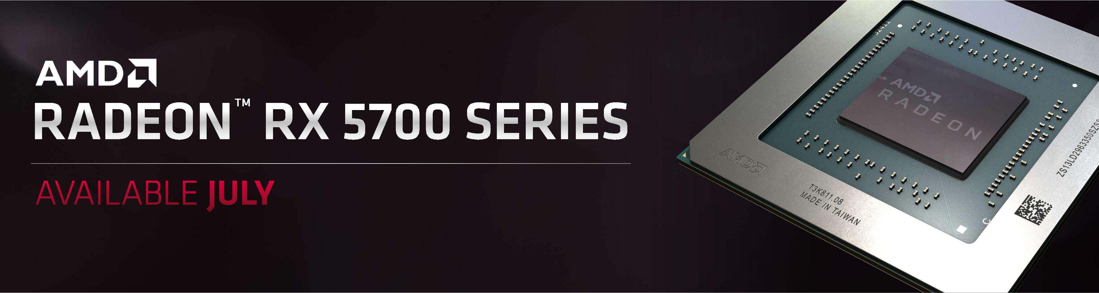
Radeon RX 5700 Series: Coming in July
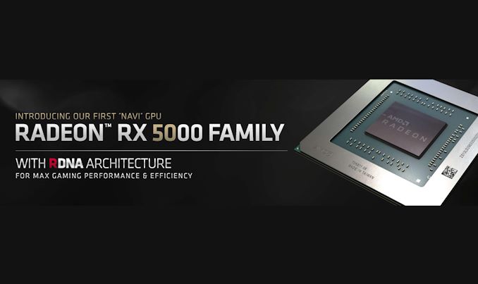
Alongside the architecture teaser, AMD also offered up some high-level details about the first Navi video cards. Navi will be sold under AMD’s RX 5000 series of video cards – that’s right, after Vega and Radeon VII, they’re going back to distinct series numbers. The RX 5000 series means that AMD is making a big jump in their numbering system, going back to 4 digits and back to the 5000 series. Officially, this is because AMD is celebrating its 50th year in business this year – so of course the product numbers need to start with a 50. However long-time observers will note that it’s been 10 years now since AMD’s previous 5000 series of video cards, the well-received Radeon HD 5000 series, and AMD may be trying to capture a bit of that.
Of the RX 5000 cards, the first series will be the RX 5700. These will be launching in July. AMD is also showing off the specific Navi GPU that will be used here, though as far as AMD’s numbering system goes, we don’t know whether this is Navi 10 or another GPU model number.
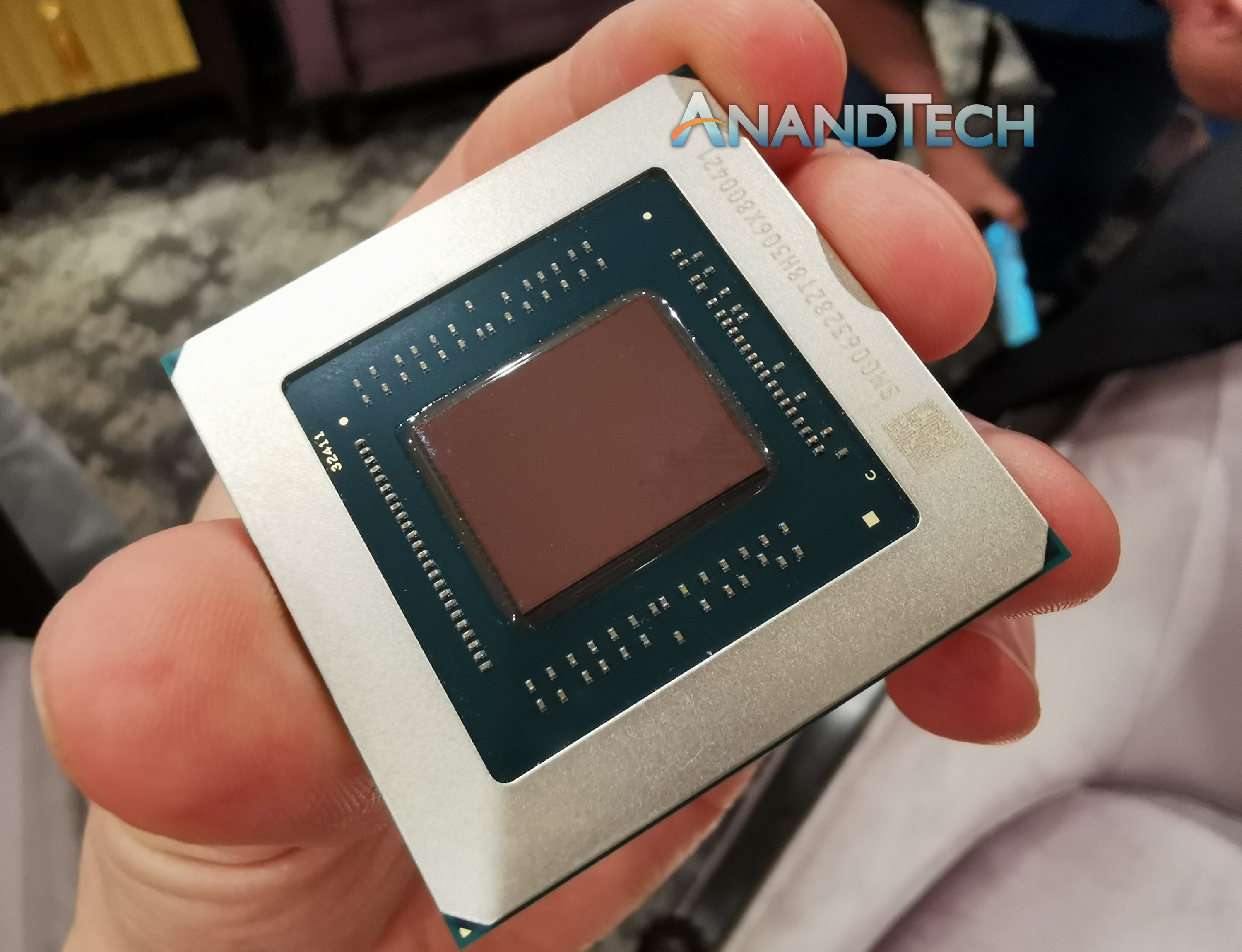
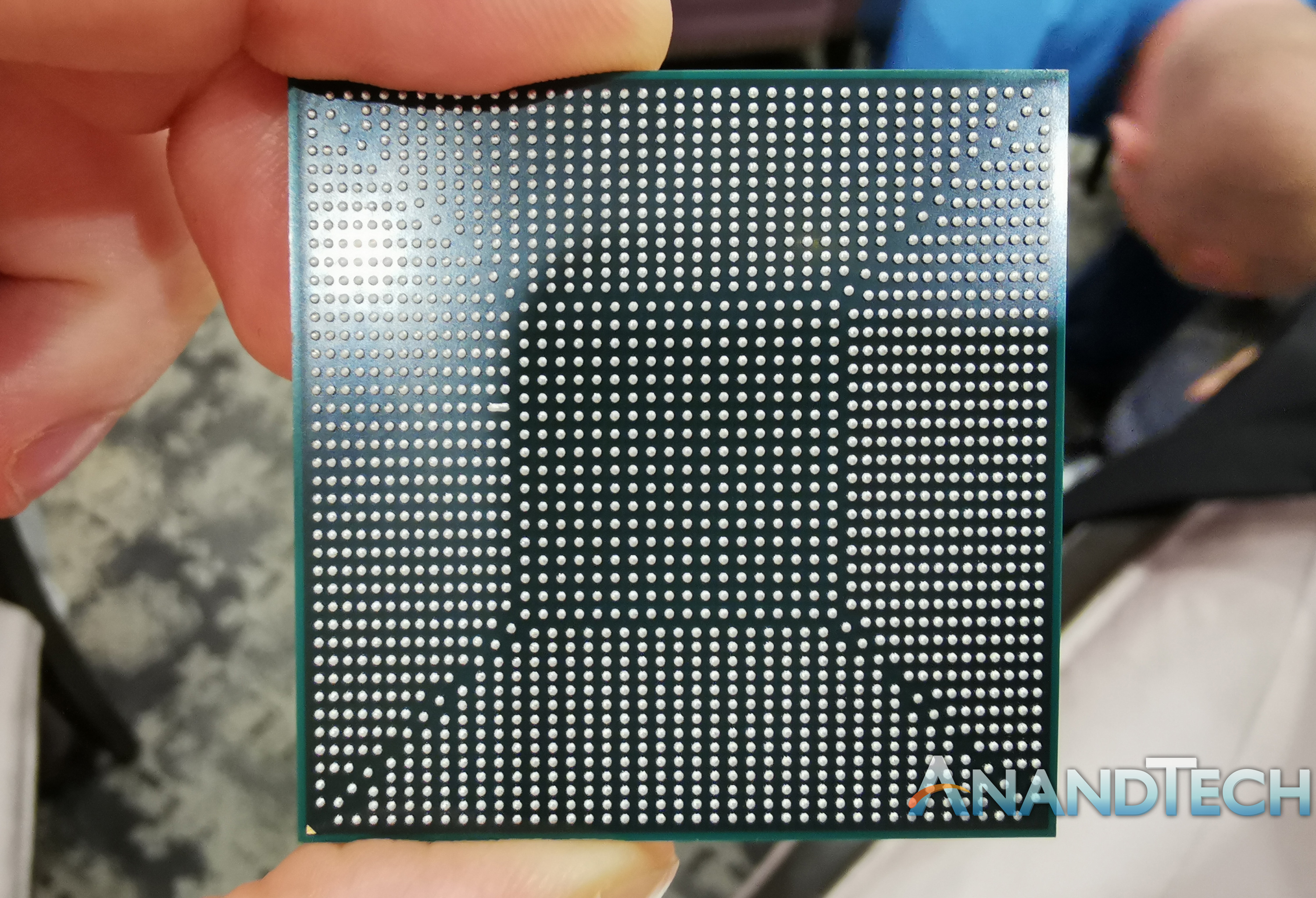
This is a traditional, monolithic die with a significant pin count package. So if I were a betting man (ed: you still owe me a steak), then I’d expect it to be paired up with GDDR6. (ed again: this has since been confirmed by AMD's press release)
Update: Thanks to our own Andrei Frumusanu for doing the leg work, we now have a die size estimate based on these and some unpublished photos. Our working guess right now is 275mm2, give or take a few percent. Though that's going to be less precise than what a proper micro-caliper measurement will turn up, so this is very much still just an estimate.
Finally, while AMD isn’t giving us concrete performance information, the company did use its Computex keynote to briefly demonstrate performance on the card versus NVIDIA’s GeForce RTX 2070, a $500 video card. While this is a game that favors AMD to begin with, it’s a promising sign that they’re able to pull ahead of mid-to-high-end NVIDIA card by 10%. Which means we’re all going to be eagerly awaiting more information on the video card as AMD ramps up for their July launch.
AMD's next big gaming event will be their E3 2019 Next Horizing Gaming Event, and AMD tells us that we'll find out more about the RX 5000 series there. So stay tuned.


99 Comments
View All Comments
gruffi - Monday, May 27, 2019 - link
"1.5x efficiency is not that high, seen the upgrade from 14nm to 7nm PP."The question is if 1.5x is the improvement of just the architecture. If so that would be really really good. If not it would be underwhelming. A new architecture and going from 12nm to 7nm should result in more than 50% better power efficiency.
CiccioB - Monday, May 27, 2019 - link
Yes, it should, but with Polaris they made even bolder statement of 2.5x (combined PP + architecture) and they resulted in a similar end case with power efficiency just barely better than GCN 1.2 and still light year behind competition, despite the new PP.So 1.5x power efficiency may still be the combination of architecture + PP as from the test they did to calculate that you cannot really estrapolate only the merits of the architecture telling them apart from those of the PP.
dr.denton - Tuesday, May 28, 2019 - link
Depends on whether you compare architectures or actual production GPUs. Polaris is very power efficient - just not at clock speeds well above 1Ghz.CiccioB - Tuesday, May 28, 2019 - link
Answered to the wrong comment below... sorryUnfortunately for AMD no GCN GPUs has ever been clocked at its sweet spot as the architecture is so computing inefficient in 3D pipeline that at the sweet spot they could just barely make competition to a two tier lower nvidia's GPUs with a not sustainable costs.
With more Hz (and consequently more W) the architecture could compete with just a tier lower nvidia GPU, so they could be sold at a loss but for much longer time.
Vega VII is the last of this series of OC GPUs with absolutely abysmal TDP with respect to their performance: Vega VII can barely beat 1080Ti consuming 100W more despite HBM and 7nm, so taking it as one of the best representative of GCN efficiency just tell how bad are the other ones.
mode_13h - Wednesday, May 29, 2019 - link
It's funny that people try to treat Vega VII as a serious consumer card. It's no more a consumer GPU than Titan V, and yet its price/perf ratio is far better.CiccioB - Wednesday, May 29, 2019 - link
Perf/price ratio is only set depending on marketing choices, not technical one.In this case AMD needs to show that it has a product that can compete with a concurrent solution that is placed under the top. The fact that it has to use a GPU thought for the computing market is by itself a sign that it is doing a marketing trick.
The facts are simple than the reasons that are brought out to justify them:
1. Polaris is now 2 generations behind the concurrent solutions
2. Vega isn't able to close the gap, despite the W and the latest expensive technology you throw at it, be them 7nm, HBM, tons of cache and bandwidth.
3. AMD has nothing to close the gap until it releases Navi, despite all the criticism about Turing and its prices (which are that level simply because AMD has nothing).
4. AMD eternal weapon is the same since the release of GCN: lower the price of its solution to match the lower tier one of the competition. At this moment it has to lower them 2 tiers to match Turing.
Despite Vega VII efficiency (which is really abysmal with respect to the PP used) , Polaris and Vega are not placed better with respect to the competition.
Krysto - Tuesday, June 11, 2019 - link
Considering it barely beats Nvidia's competing products on 14nm, I'm going to assume the 1.5x efficiency is from the 7nm node alone.mode_13h - Wednesday, May 29, 2019 - link
> I have now counted at least 4 cache hierarchy redesign in AMD architectures. It seems they are not able to use caching appropriately and keeps on experimenting on it. Hope this is the right scheme.It's funny that you pose this as a matter of correctness. At least some of those changes were probably driven by priorities among their target markets and their needs. Others were probably enabled by technological changes, such as Infinity Fabric, HSA, and HBM.
CiccioB - Wednesday, May 29, 2019 - link
These are only guesses that try to find other justifications about AMD (un)skill in creating GPU architectures.Some may be or not, whatever: what I see is that their cache schemes have varied in time on the same architecture (GCN) with no other technical changes but the fact that the previous choices were wrong.
- IF is not used for the GPU, so it is useless to induce it as a possibile reason
- HSA is a waporware thing that only work with iGPU as there are no example on where it has been applied with some advantage. Be it a reason for it, one may wonder why L2 cache and ROPs access changed (ROPs have nothing to do with HSA).
- HBM is used on a particular designed architecture so if ever that architecture should have been used with such modifications, but we see modification done on GDDRx architectures.
All I can see is AMD changing the cache hierarchy layout now and then saying that the changes is going to make improvements which however we do not see at all.
nvidia is keeping their cache hierarchy the same way it was from Kepler, so probably they created a better thought architecture to evolve since 2012. And as a result of this after 7 years we have Turing from nvidia which goes beyond the classic rasterization fixed units and a rebranded shrunk Vega without RT/tensor/advance geometry from AMD which is still thinking if it better to link ROPs directly to L2 or go directly to VRAM.
AndrewJacksonZA - Monday, May 27, 2019 - link
"(ed: you still owe me a steak)"*chuckle * I really enjoy the personality that shows through in this site. I like the culture here. :-)