Hands on with the 56-core Xeon Platinum 9200 CPU: Intel’s Biggest CPU Package Ever
by Ian Cutress on April 8, 2019 11:00 AM EST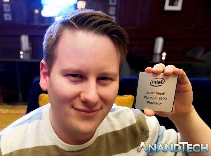
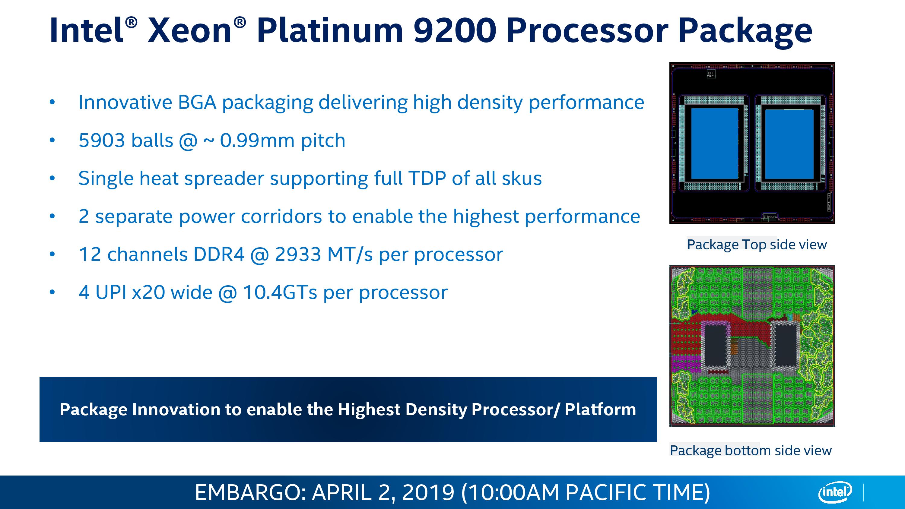
When Intel announced the new Cascade Lake family as officially launched last week, it added a new product segment to its portfolio – the ‘Advanced Performance’ or AP. These come in the form of the Xeon Platinum 9200 family, and feature two of Intel’s high-end processors within a single package, offering double the cores and double the memory in a much denser environment. These processors are focusing purely on density, and are BGA only so they will only be sold as complete systems by OEMs, who actually buy them from Intel and make modifications. We had the opportunity to hold one of these big CPUs and take some pictures.
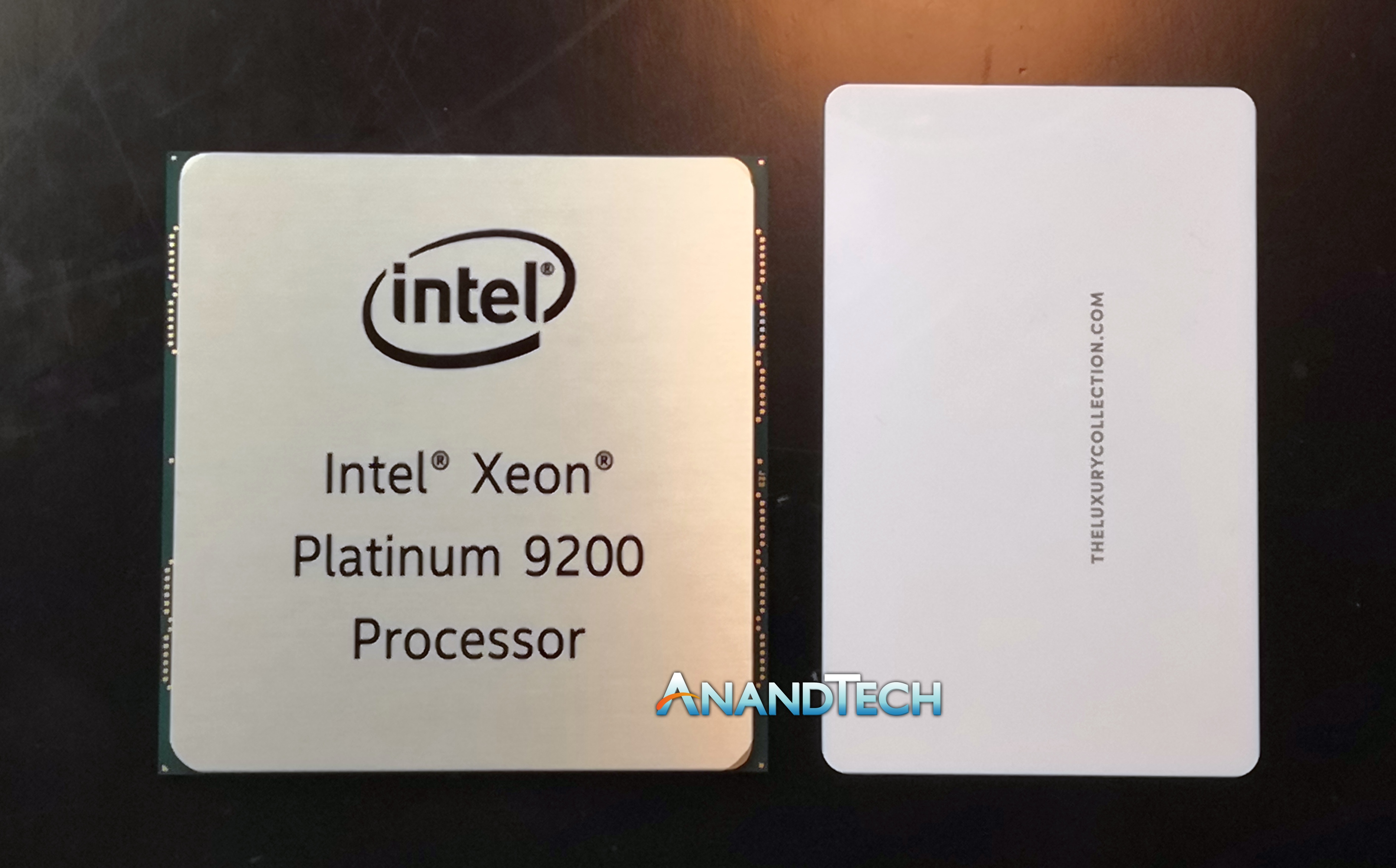
The package measures 76.0 x 72.5 mm, making it Intel’s largest CPU based* package ever, beating out the old Intel Pentium Pro, which was 67.6 x 62.5 mm, and AMD’s EPYC package, which is 75.4 x 58.5 mm.
Source: Intel
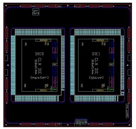
Inside the package is two XCC enabled silicon die, one designated a master, and one a slave. The die themselves are ~694mm2 each.
The Biggest Baller In The Park
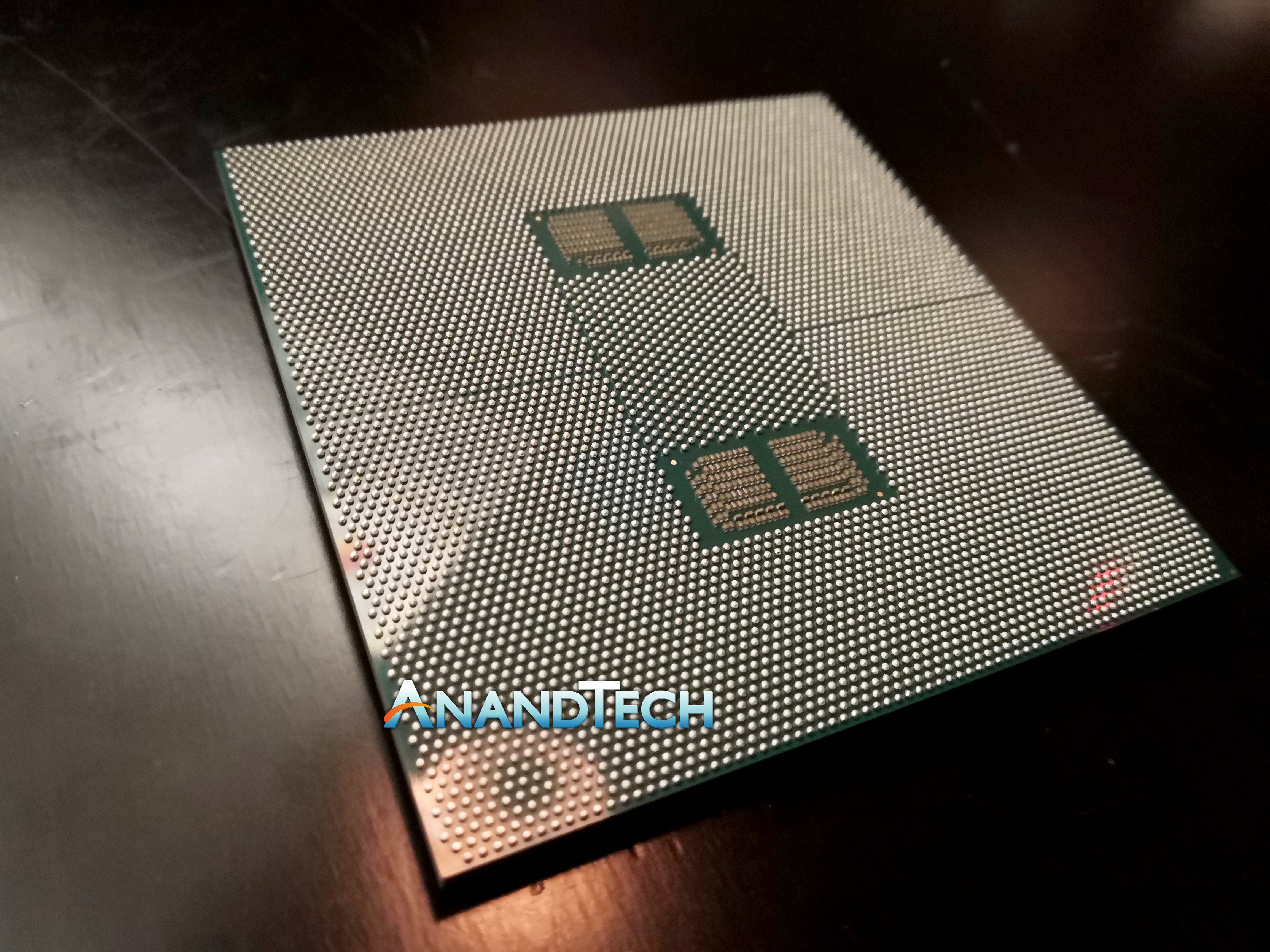
The socket is officially called FCBGA5903, which stands for flip-chip ball-grid array 5903, with 5903 being the number of contacts or ‘balls’ on the underside which goes onto the motherboard, much like an embedded chip. By contrast, AMD’s EPYC chip has 4094 pins. The reason for all these contacts are mostly in the memory: as this Platinum 9200 processor has twelve memory channels, these all require pins. There are also some more for power, as the TDP for the 56-core version is 400W.
To begin, Intel is offering four different types of Platinum 9200:
| Intel Xeon Platinum 9200 Family (Cascade Lake AP) |
||||||
| AnandTech | Cores | Base Freq |
Turbo Freq |
L3 Cache |
TDP | Price |
| Platinum 9282 | 56 C / 112 T | 2.6 GHz | 3.8 GHz | 77.0 MB | 400 W | head |
| Platinum 9242 | 48 C / 96 T | 2.3 GHz | 3.8 GHz | 71.5 MB | 350 W | shoulders |
| Platinum 9222 | 32 C / 64 T | 2.3 GHz | 3.7 GHz | 71.5 MB | 250 W | knees |
| Platinum 9221 | 32 C / 64 T | 2.1 GHz | 3.7 GHz | 71.5 MB | 250 W | toes |
In terms of weight, the processor is definitely around 200-300g, or half a pound. This was measured very scientifically by comparing it in my hands to the weight of my heaviest phone, and then comparing it to two phones. The chip certainly has some hefty bulk, but given that it is a BGA design, it’s unlikely that even people using the chip will ever hold it.

If we look side on to the design, we can see that the package actually has three distinct layering stages (five, if you include the caps). The light brown and dark brown layering totals up to 18 layers (recorded by eye, hard to see in difficult light), and the dark brown layers are clearly double the thickness of the light brown layers, which might indicate that these are the power planes of the package. Normally we see processors with anywhere from 8-12 layers total, so this is another step up above that.

A close up of the ball array shows the fine pitch between the contacts. The capacitors on the underside are extremely tiny in comparison to other CPUs - I mean really small. Each of these corners has 87 capacitors, making for a total of 348.
Pricing for this family of processors is not expected to be disclosed. Intel has stated that as they are selling these chips as part of barebones servers to OEMs that they will unlikely partition out the list pricing of the parts, and expect OEMs to cost them appropriately. Given that the new high-end Intel Xeon Platinum 8280L, with 28 cores and support for 4.5 TB of memory, runs just shy of ~$18k, we might see the top Xeon Platinum 9282 be anywhere from $25k to $50k, based on Intel margins, OEM margins, and markup.

nom nom nom, chips
*Intel may have FPGA products that exceed this size, mainly due to HBM and other chiplets on board.


Related Reading
- Intel's Enterprise Extravaganza 2019 Roundup
- Intel Xeon Scalable Cascade Lake: Now with Optane!
- Intel Agilex: 10nm FPGAs with PCIe 5.0, DDR5, and CXL
- Intel Columbiaville: 800 Series Ethernet at 100G, with ADQ and DDP
- Intel Launches the Xeon D-1600 Family: Upgrades to Xeon D-1500
- Lenovo’s New Cascade Lake ThinkSystem Servers: Up to 8 Sockets with Optane
- Dell PowerEdge Updates: Upgrade to Cascade Lake and Optane
- Supermicro Calvinballs Into Cascade Lake: Over 100 New and Updated Offerings


66 Comments
View All Comments
Ninjawithagun - Thursday, June 13, 2019 - link
Wow, you are a sore loser. Don't fret and be pissed just because Intel got fat and lazy. AMD has not only caught up, but has surpassed them. There is no reverse engineering whatsoever. The Ryzen CPUs have a completely different architecture. Do you even know what the hell you are talking about? Yup, didn't think so!3ogdy - Saturday, May 30, 2020 - link
Nice try, but...Ring bus vs Infinity Fabric. The way each operates, from the architecture, the principle and the links to different system components (RAM clock speed in the case of IF) prove you are wrong. Zen is not an Intel architecture that was reverse engineered. It was built from the ground up. No wonder Intel had to get AMD's engineers to try and become competitive again.StevoLincolnite - Monday, April 8, 2019 - link
10 years ago you could get the Core i7 870. 2.93Ghz, Quad-Core.6~ months later you could get the Core i7 970. 3.2Ghz, Hex-Core. - This chip still stands up really well even today, especially once overclocked... Mostly thanks to the extra threads which translates well to newer titles.
ballsystemlord - Monday, April 8, 2019 - link
Could you please tell me how the Zen core is related to Intel's I7s? I'm at a total loss, unless you conclude that the performance is similar and, therefore, it much be a reverse engineered I7!Samus - Tuesday, April 9, 2019 - link
Some people draw clueless similarities between Zen and Core because Zen has trivial things like Jackson Technology (hyper threading) and a similar implementation of turbo boost\speed step that controls voltage and clock speed together.Architecturally they are entirely different, just look at a pipeline diagram they have little in common. The result is Zen is more efficient per clock, resulting in less energy usage to calculate the same arithmetic before specific optimizations. And the optimizations are where things have historically benefited Intel.
I just build a massive DVR for a client that records h264 video streams from a dozen 4k cameras at 15fps. It is incredibly CPU intensive and AMD seemed the natural choice since rendering is often favorable for AMD. Except AMD CPU's don't have any implementation of QuickSync - an Intel GPU + CPU encoding engine that uses the GPU EU's to lossy compress video with negligible impact on video quality. The catch is it doesn't support h265 which is more space-efficient but the fact a dozen cameras are EASILY handled by a Core i7-8700 6-core CPU (averaged 30% CPU load) when even the most powerful Ryzen 2800x 10-core CPU struggled with a dozen cameras (averaged 80% CPU load) left the AMD solution with no headroom for growth and a substantially higher power budget.
Goes to show how important optimizations. If a program DIDN'T take advantage of QuickSync then AMD would likely be the clear victor here, but the lack of extensions in various scenarios hurts them.
Alexvrb - Tuesday, April 9, 2019 - link
The first SMT design was the never-released DEC EV8. Tullsen's work later made it into the P4.Also QuickSync is yet another proprietary and limited tech, and not an actual extension of x86-64. Quality of the resulting encodes is mediocre and it supports limited profiles (and no custom profiles). That doesn't even count the aforementioned lack of codec support. So from my perspective it's not useful at all. However for your client it's good because I'm sure they don't need perfect quality / max bitrate savings, just good enough and lots of video.
With that being said, it may not have as much headroom as you think. How many streams can QuickSync accelerate? What if they want to use a newer codec to save space down the road like HEVC, AV1, VVC? H.264 AVC is really not that efficient at 4K. Also, 2800X, 10 core? Have you been smoking the crack again?
Budburnicus - Wednesday, October 14, 2020 - link
Uhhhh.... You mention a Ryzen 2800X - this does NOT exist. Neither does ANY 10 Core AMD CPU!You may be right about recording and all, but your knowledge of Ryzen is suspect. There is NO Ryzen, Threadripper, or EPYC CPU with exactly 10 cores...
(I have an 8700k @ 5.1 GHZ for my gaming machine m8, but I know Ryzen specs.)
bobhumplick - Monday, April 8, 2019 - link
if youre going to fanboy then at least put some thought into itballsystemlord - Monday, April 8, 2019 - link
Good point. Let's call it: Cascade-dozer. :)Seriously, when it comes to criticism doesn't it ever seem to you that people tend to the lowest common denominator (Fail-dozer [1]) in order to spread the message to the absolute maximum amount of people?
If you really wanted to say something how about quoting Intel? "Inconsistent Performance from 2 Glued-together Desktop Die" [2]
And, in the same vein, if you wanted to say something intelligent how about, "Gee, upgrading or replacing those CPUs is going to be difficult or beyond the average IT guy."?
Or how about something witty, "It does not include the Nuclear reactor that powers the CPU?!",
Or, if you preferred both, "Ah, another CPU that requires only a 4 phase MB!"
Go ahead, throw us a bone instead of equally dumb criticism.
[1] http://en.linuxreviews.org/AMD_Faildozer
[2] https://www.techpowerup.com/img/QhA6gdonrmBT27fr.j...
yeeeeman - Thursday, August 8, 2019 - link
I do agree that current Intel efforts are unlike what they had in the past. I do agree that most of the stuff they get on the market in past two years feels like an afterthought. It might very well be, since they probably had some plans with 10 and 7nm processes and all of them became unfeazable when 10nm turned out to be broken.Still, I think we should give kudos to Intel because given all the shitty fab situation, they managed to find ways to improve stuff, ON THE SAME NODE. Sure, they can defy the laws of physics, so power consumption is high, but then again, remember that AMD was in the same place a few years ago with 32/28nm processes. They couldn't make anything remotely worthy of competing with Intel. Sure, they optimized power consumption in various ways, but they were still rubbish.
Lets be fully honest. When you're stuck on the same node, that is when you MUST get creative. And surely so, Intel did bump up the clocks to absurd levels on desktop parts, while keeping - sort of - things in check. They do still compete on performance, so I think that is testament to how good they uArch was and still is. On the server side, things are more tricky, since cost is a big part of the picture. Because of Intel internal layout of the chip, they can't really split it easily into many chiplets without losing the low latency advantage. Also, making huge dies, while making money on them (taking into consideration yields) is VERY difficult. AMD has a lot of cards in their hands now with the server parts and Intel desperately needs a good fab process, Ice Lake with that 20% IPC improvement and a higher core count die (say 40 cores). That would bring them close to the 64 cores of AMD from a performance pov.
Anyhow, things are quite interesting these days in the world of CPUs and I am happy that Intel will work their asses to get back to speed again.