Intel's Basin Falls Skylake-X Refresh: Core i9-9980XE with up to 15% Better Power Efficiency
by Ian Cutress on October 8, 2018 10:50 AM EST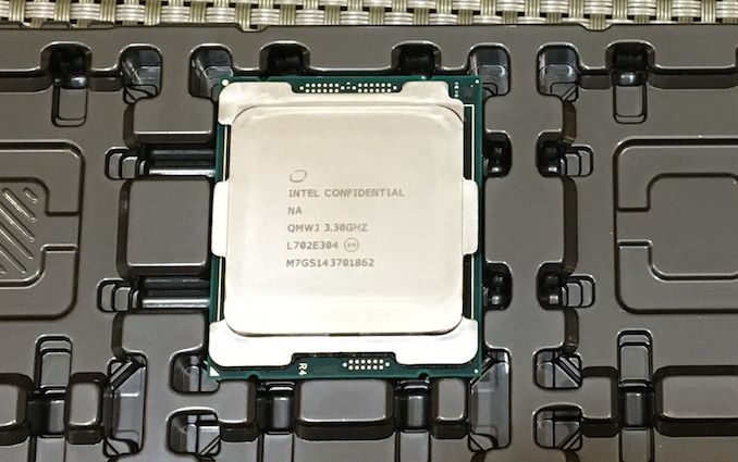
One of the interesting things about Intel’s latest generation of high-end desktop parts was the jump from ten cores at the peak to eighteen, as Intel moved its high core count Skylake-X die into the consumer market. This meant more cores, at a higher cost, and now Intel had seven different HEDT processors rather than three or four. Today Intel is releasing information about an update to this platform: seven new processors, with higher frequency, and as an added kicker, there’s something funny going on with the cache.
A Quick Refresher: Intel’s Large CPU Silicon
At the high-end of Intel’s processor product line, it produces processors for both high-performance enterprise and high-end desktop (HEDT). In order to create a wide range of products with its technology, and attract higher margins, Intel makes three different dies of various sizes based on their total core count:

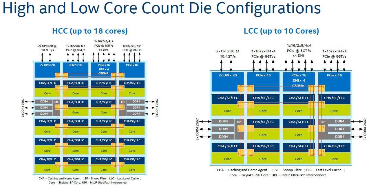
These three floor plans are called LCC (low core count), HCC (high core count), and XCC (extreme core count). By having three different sizes, Intel optimizes its manufacturing: the 10-core LCC die is smaller, and can be enabled/disabled to make 4-10 core products; the 18-core XCC die is focused more on the mid-range, and the 28-core XCC goes for the big money. Very few customers want a 4-core from a 28-core die, so this helps maximize processors per wafer, and Intel keeps its costs down.
That being said, on the enterprise Xeon processor line, there are some chips with odd properties. For example, Intel can disable cores but keep the L3 cache of that core active: a 24 core part could have access to 28 cores' worth of L3 cache. This extra cache has added latency (as does accessing L3 cache on another CPU), and there are considerations on how the power is managed on the chip which affects TDP.
The reason why I’m bringing this up is because of what Intel is announcing today. For the Skylake-X HEDT platform, Intel used its LCC die for the 6-10 core products, and HCC die for 12-18 core products. With this new refresh, called Basin Falls Refresh or Skylake-X Refresh (SLX-R?), it would appear that every processor is from the HCC family. We can see this because of the cache sizes.
More Cores, More CPUs, More Cache
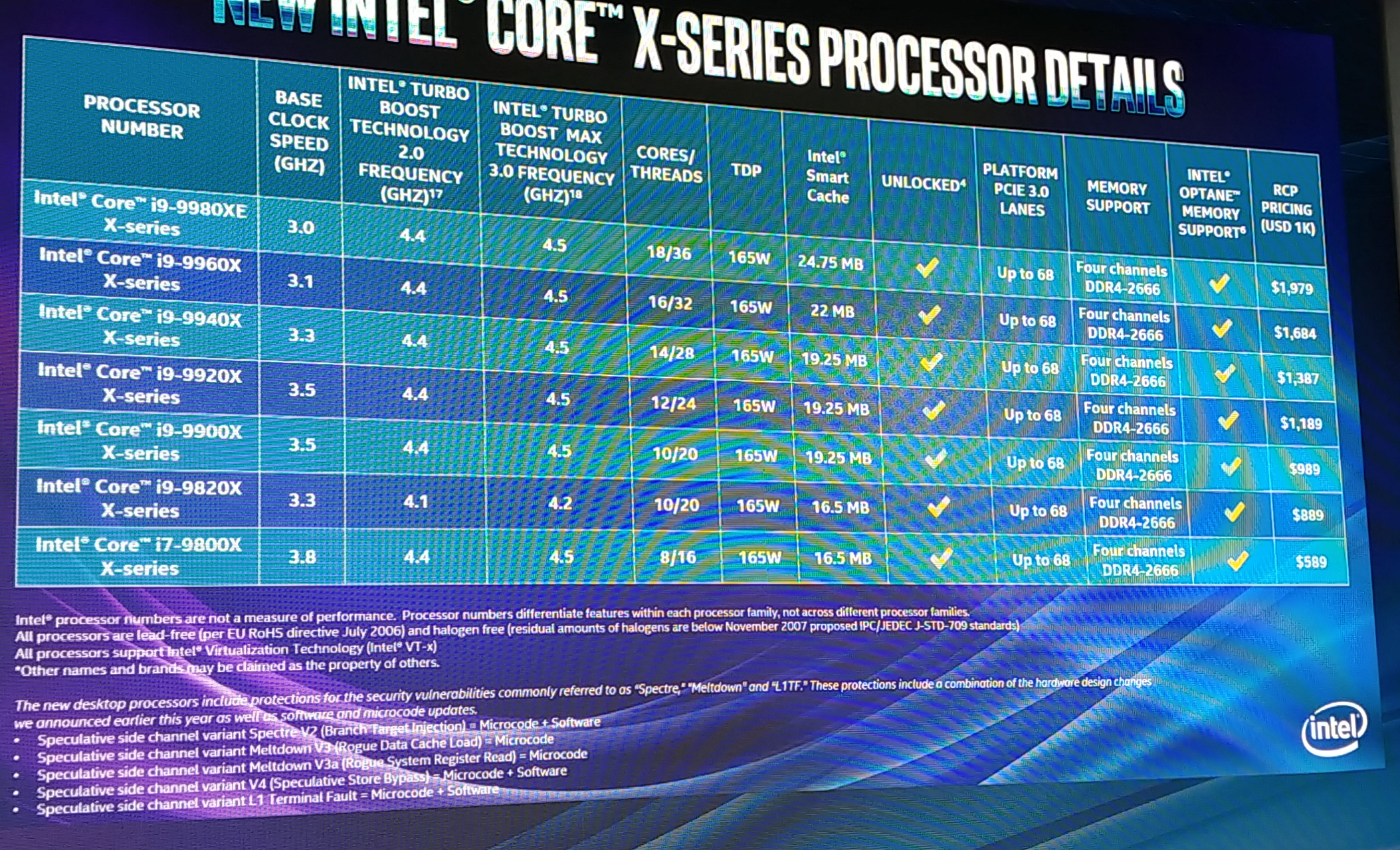
Today Intel is announcing seven new CPUs for the LGA2066 socket / X299 platform, ranging from 8 cores to 18 cores.
| Intel Basin Falls Skylake-X Refresh | ||||||||
| AnandTech | Cores | TDP | Freq | L3 (MB) |
L3 Per Core |
DRAM DDR4 |
PCIe | |
| i9-9980XE | $1979 | 18 / 36 | 165 W | 3.0 / 4.5 | 24.75 | 1.375 | 2666 | 44 |
| i9-9960X | $1684 | 16 / 32 | 165 W | 3.1 / 4.5 | 22.00 | 1.375 | 2666 | 44 |
| i9-9940X | $1387 | 14 / 28 | 165 W | 3.3 / 4.5 | 19.25 | 1.375 | 2666 | 44 |
| i9-9920X | $1189 | 12 / 24 | 165 W | 3.5 / 4.5 | 19.25 | 1.604 | 2666 | 44 |
| i9-9900X | $989 | 10 / 20 | 165 W | 3.5 / 4.5 | 19.25 | 1.925 | 2666 | 44 |
| i9-9820X | $889 | 10 / 20 | 165 W | 3.3 / 4.2 | 16.50 | 1.650 | 2666 | 44 |
| i7-9800X | $589 | 8 / 16 | 165 W | 3.8 / 4.5 | 16.50 | 2.031 | 2666 | 44 |
| Skylake-X | ||||||||
| i9-7980XE | $1999 | 18 / 36 | 165 W | 2.5 / 4.4 | 24.75 | 1.375 | 2666 | 44 |
| i9-7960X | $1699 | 16 / 32 | 165 W | 2.8 / 4.4 | 22.00 | 1.375 | 2666 | 44 |
| i9-7940X | $1399 | 14 / 28 | 165 W | 3.1 / 4.4 | 19.25 | 1.375 | 2666 | 44 |
| i9-7920X | $1199 | 12 / 24 | 140 W | 2.9 / 4.4 | 16.50 | 1.375 | 2666 | 44 |
| i9-7900X | $999 | 10 / 20 | 140 W | 3.3 / 4.5 | 13.75 | 1.375 | 2666 | 44 |
| i7-7820X | $599 | 8 / 16 | 140 W | 3.6 / 4.5 | 11.00 | 1.375 | 2666 | 28 |
| i7-7800X | $389 | 6 / 12 | 140 W | 3.5 / 4.0 | 8.25 | 1.375 | 2400 | 28 |
These are direct replacements for the current Skylake-X processors, except for the lack of a six-core processor which is lost because the mainstream consumer platform now goes up to eight processors.
The key highlights in the table are listed in bold. All the new processors have a new TDP of 165W, which is the TDP of the old HCC processors. All the processors have significant bumps in base frequency compared to the previous generation, with the old 165W chips getting bumps of up to 400 MHz, showing what should be a 15% increase in power efficiency. For the processors moving up from 140W to 165W, there is up to a 600 MHz jump in base frequency, taking advantage of both the power efficiency increase and the TDP increase. All the turbo frequencies are up to 4.5 GHz except the lower-tier 10 core part. Also worth noting is that every processor now offers 44 PCIe lanes.
A combination of the TDP and the lane count would suggest that each of the CPUs is now built from the HCC die. But the other element is the L3 cache.
For the Skylake-X microarchitecture, each CPU has 1.375 MB of L3 cache – so a 10 core CPU should have access to 13.75 MB. If we take the culprit that has changed the most – the 10-core Core i9-9900K – it should have 13.75MB, but it actually has 19.25MB, which is what a 14 core CPU would get. So underneath the heatspreader, the Core i9-9900K is at least a 14-core part. Because Intel has only made 10/18/28 core silicon for this platform, it means that underneath, it is the 18-core, or HCC part.
But what does this mean for performance? On paper, probably not a lot.
The L3 cache in these parts is a non-inclusive, victim cache. This means that it cannot accept data direct from DRAM, and only contains data that has been loaded into L2 then kicked out into the L3 cache, whether it was used or not. The L3 benefits workloads that has repeat data accesses on immediately close-by data, which is very few consumer oriented workloads (typically integrated graphics gaming, or compression). So while more cache is a good thing, based on previous experience, the performance uplift is unlikely to be more than a percentage point at best in general.
No More 28 PCIe Lane Neutering
For me, one of the biggest highlights of the updated processor line is the PCIe lane count. Rather than having the cheaper models with 28 lanes and the more expensive models with 44, Intel has gone back to having everything with 44 lanes. This makes motherboard deciphering much simpler, and allows everyone to support PCIe storage direct from the CPU, rather than through the chipset which can be bottlenecked upstream by the CPU-to-chipset link.
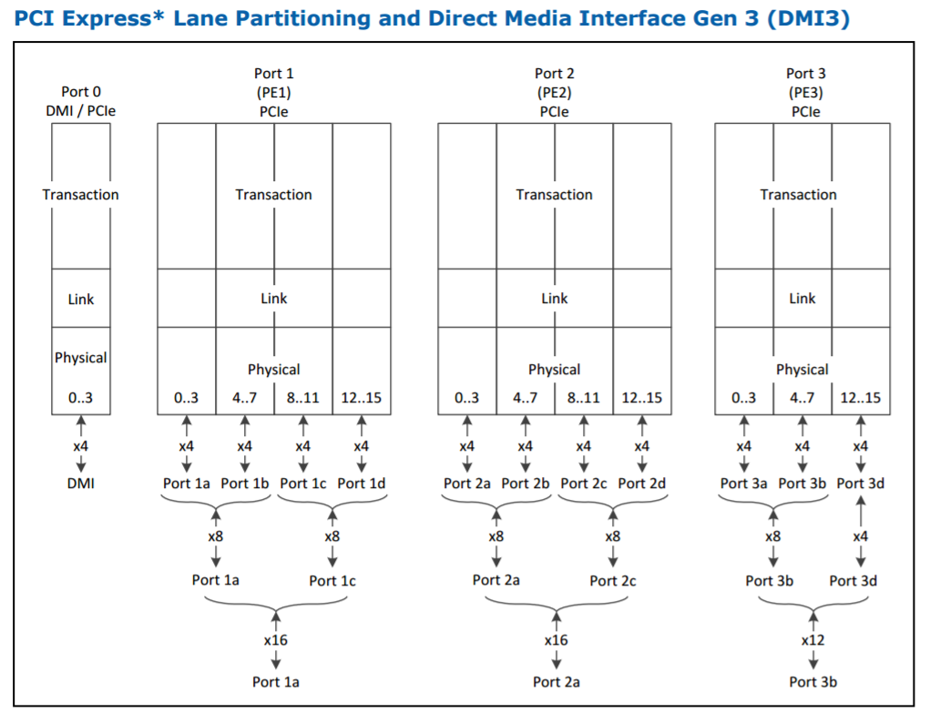
How 44 Lanes are Partitioned, Plus DMI
It also benefits multi-GPU arrangements, or any multiple accelerator, or for users that want to add in Thunderbolt 3 cards, or multi-gigabit Ethernet, or development on FPGAs, or... (you get the idea) Readers will point to the fact that Intel’s HEDT is now competing against AMD’s Threadripper 2 platform, which has 60 PCIe lanes, as a factor in Intel’s decision in order to remain competitive on this front. The biggest use for the large PCIe lane count in AMD’s enterprise lineup so far is in storage, so it will be interesting to see how it plays out in the consumer space.
How Did Intel Gain 15% Efficiency? Design? Solder?
If we take the Core i9-9980XE flagship processor, the base frequency for this 18-core part has increased from 2.6 GHz to 3.0 GHz, or around 15.4 %. The TDP is listed as 165W, and as a reminder, Intel always relates the TDP to the base frequency, not the turbo frequency (the power consumption under turbo can be much higher). So it would imply that Intel has done something to increase the processor's efficiency.
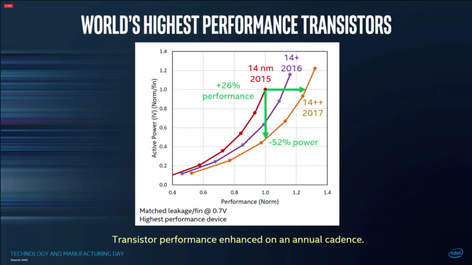
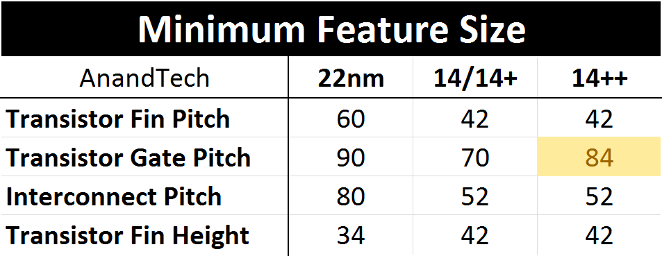
The simplest answer would be that Intel is now manufacturing these parts on its 14++ process node, which Intel now calls part of its ‘14nm class family’. The 14++ node is a slightly relaxed version of 14+, with a slightly larger transistor gate pitch:
This relaxing of feature size usually does two things: it allows for a higher frequencies, but it can also lead to increased power consumption. The move from 14+ to 14++ may have required new manufacturing masks as well, depending if Intel is keeping the same layout as the original Skylake-X. Using new masks incurs additional costs, but also allows Intel to make some changes in the chip that might help track voltage closer to the cores for better efficiency. At the time of writing, we’re waiting to hear exactly what security changes (if any) have been applied, and this will depend on if Intel had to redesign its masks for 14++.
The other angle to this is the bonding between the CPU and the heatspreader. While this doesn't lead directly to an efficiency increase, it does help reduce the heatsoak and technically puts less pressure on the TDP. TDP is the Thermal Design Power, and essentially the metric that states that the cooler needs to be able to dissipate 165W. The power consumption of the system can be larger, due to thermal losses through the socket, but usually the two are considered equal.
Having solder in there, instead of thermal paste like the previous generation, helps move those thermals away from the CPU, giving it additional headroom. It also arguably puts less pressure on the cooler materials, reducing the pressure on TDP. At the time of writing, the use of solder hasn't been confirmed, but it would be a very good idea for Intel to do this, especially on a platform with few other changes.
Motherboards: Keeping the X299
Unlike the Z390 launch with the new Core-S processors, motherboard manufacturers have been relateively quiet for this refresh as there isn't a new chipset to generate a full stack of products. Normally we see one or two manufacturers launch refresh models, updated for the power consumption increases or with added new features, but before writing this, no manufacturer has approached us with information on new models.
This means the state of play on X299 will stay the same, albeit with BIOS updates required. It will be a while before the boards on shelves will be automatically updated for sure, meaning that people buying new into the system might have to double check with the retailer that the board they purchase is already updated (or purchase a board with an offline update feature with no CPU present).
For users interested, we have a deep history in our X299 reviews to flick through:
- The MSI X299 XPower Gaming AC Review: Flagship Fantasy
- The ASRock X299 Extreme4 Motherboard Review: $200 Entry To HEDT
- The MSI X299 Gaming M7 ACK Motherboard Review: Light up the Night
- The ASUS Prime X299-Deluxe Motherboard Review: Onboard OLED and WiGig
- The EVGA X299 Micro Motherboard Review: A Smaller Take on X299
- The EVGA X299 FTW K Motherboard Review: Dual U.2 Ports
- The GIGABYTE X299 Gaming 7 Pro Motherboard, Reviewed
- The ASUS ROG Strix X299-XE Gaming Motherboard Review: Strix Refined
- The ASUS TUF X299 Mark I Motherboard Review: TUF Refined
- The MSI X299 SLI Plus Motherboard Review: $232 with U.2
- The MSI X299 Tomahawk Arctic Motherboard Review: White as Snow
- The ASRock X299 Taichi Motherboard Review
- The ASRock X299 Professional Gaming i9 Motherboard Review
- The MSI X299 Gaming Pro Carbon AC Motherboard Review
Our X299 coverage is our largest of a motherboard platform in recent memory, so check it out. Joe did some great work!
So Who Is This Aimed At?
If the CPU microarchitecture is fundamentally the same, it has the same memory support, and most of the middle-range features are upgraded to a better minimum level, who exactly is this launch aimed at? Intel often cites the 'mega-taskers' as its main audience here - the users that both stream, edit video, and play video games concurrently, or others that compile and test but also have 50 other things on the go. That's the target market, but who would be upgrading to this?
Despite the supposed 15% better performance efficiency (or better thermals), I don't invisage users upgrading from a Core i9-7980XE (or any Skylake-X processor) to this unless they can justify the cost. The HEDT customer is interested in might be on a Sandy Bridge-E or Haswell-E system already, or something like a mainstream Ryzen, and looking for more grunt. That's where the available market is to be honest.
Timeline for Skylake-X Refresh
Today is only the announcement for the new processors – Intel isn’t giving firm dates on when they are coming to the market at the time of writing, but we expect to see them within the next month or so. When it comes to pricing, the “entry level” Core i7-9800X will cost $589. Meanwhile, the ultra-high-end Core i9-9980XE carries an MSRP of $1,979, which is in line with the price of its direct predecessor. Pricing of other “extreme” CPUs are somewhere between, as you can see in the table above and on the slide below. Meanwhile, given the increase of frequencies, the new products are priced higher than their predecessors.


31 Comments
View All Comments
ianken - Friday, November 2, 2018 - link
Late to this but: I'm curious to see 9800x vs 9900k perf. Higher boost vs. fatter cache and more memory bandwidth...