MediaTek Announces New Premium Helio P60 SoC
by Andrei Frumusanu on March 1, 2018 9:30 AM EST- Posted in
- Smartphones
- Arm
- Mobile
- Trade Shows
- MediaTek
- Mali
- Helio
- MWC 2018
- P60
- A73
- A53
- ARM Cortex
BARCELONA, ESP – Earlier this week MediaTek announced a new entry in the Helio SoC line-up, the Helio P60. The P60 comes with a strategy change for MediaTek as the company is doubling down on the super-midrange “premium” category and expanding that range into multiple sub-tiers.
The strategy change comes from market and lack of success in the high-end Helio X series. Last year’s Helio X30 had only a few design wins and was relatively late to market. MediaTek seems to have had a string of bad luck with the X20 and X30 as both came on either problematic or very delayed manufacturing process nodes which lost them important design wins. As more vendors switch over to custom designs in the high-end and Qualcomm puts more pressure with competitive designs, MediaTek decided to put a hold on the X series for now and concentrate in the range where it is very successful, the P series.
The this new segmentation means that the P60 doesn’t position itself as direct successor to late last year’s P23 and P30 but rather as a tier above them, hence the naming scheme.
| MediaTek Current P-Series | |||
| SoC | Helio P23 | Helio P30 | Helio P60 |
| CPU | 4x Cortex A53 @ 2.3GHz 4x Cortex A53 @ 1.65GHz |
4x Cortex A53 @ 2.3GHz 4x Cortex A53 @ 1.65GHz |
4x Cortex A73 @ 2.0GHz 4x Cortex A53 @ 2.0GHz |
| GPU | Mali G71MP2 @ 770MHz | Mali G71MP2 @ 900MHz | Mali G72MP3 @ 800MHz |
| APU / NPU / AI Proc. / Neural IP | - | 2x 140GMACs | |
| Memory | 1x 32bit LPDDR3 @ 933MHz 2x 16bit LPDDR4X @1500MHz |
2x 16bit LPDDR4X @ 1600MHz | 1x 32bit LPDDR3 @ 933MHz 2x 16bit LPDDR4X @ 1800MHz |
| ISP/Camera | 1x 24MP or 2x 13MP | 1x 25 MP or 2x 16MP | 1x 32MP or 2x 20+16MP |
| Encode/ Decode |
2160p30 H.264 | 2160p30 H.264 & HEVC | 2160p30 H.264 & HEVC |
| Integrated Modem | Category 6 DL = 300Mbps 3x20MHz CA, 64-QAM UL = 50Mbps 64-QAM |
Category 7/13 DL = 300Mbps 3x20MHz CA, 64-QAM UL = 150Mbps 2x20MHz CA,64-QAM |
Category 7/13 DL = 300Mbps 3x20MHz CA, 64-QAM UL = 150Mbps 2x20MHz CA,64-QAM |
| Mfc. Process | 16FFC | 16FFC | 12FFC |
The P60 is the first SoC in the P-lineup to employ “big” microarchitecture cores as it uses 4x Cortex A73 cores at up to 2.0GHz – a significant performance boost in performance over the P23 and P30’s A53 cores. The efficiency cores are naturally still Cortex A53’s and they run at the same 2.0GHz frequency as the performance cluster.
On the GPU side we see an update in the IP as MediaTek in turn transitions from G71 to G72. The P60 uses a G72MP3 running at up to 800MHz and promises a 25% gaming efficiency boost (at up to 70% higher GPU performance).
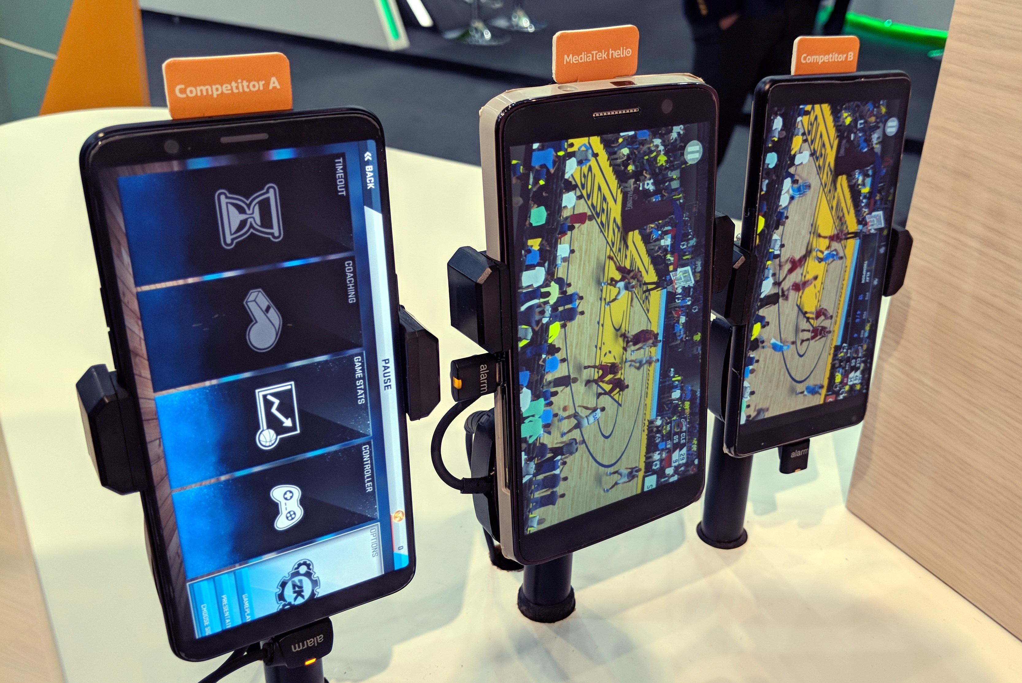
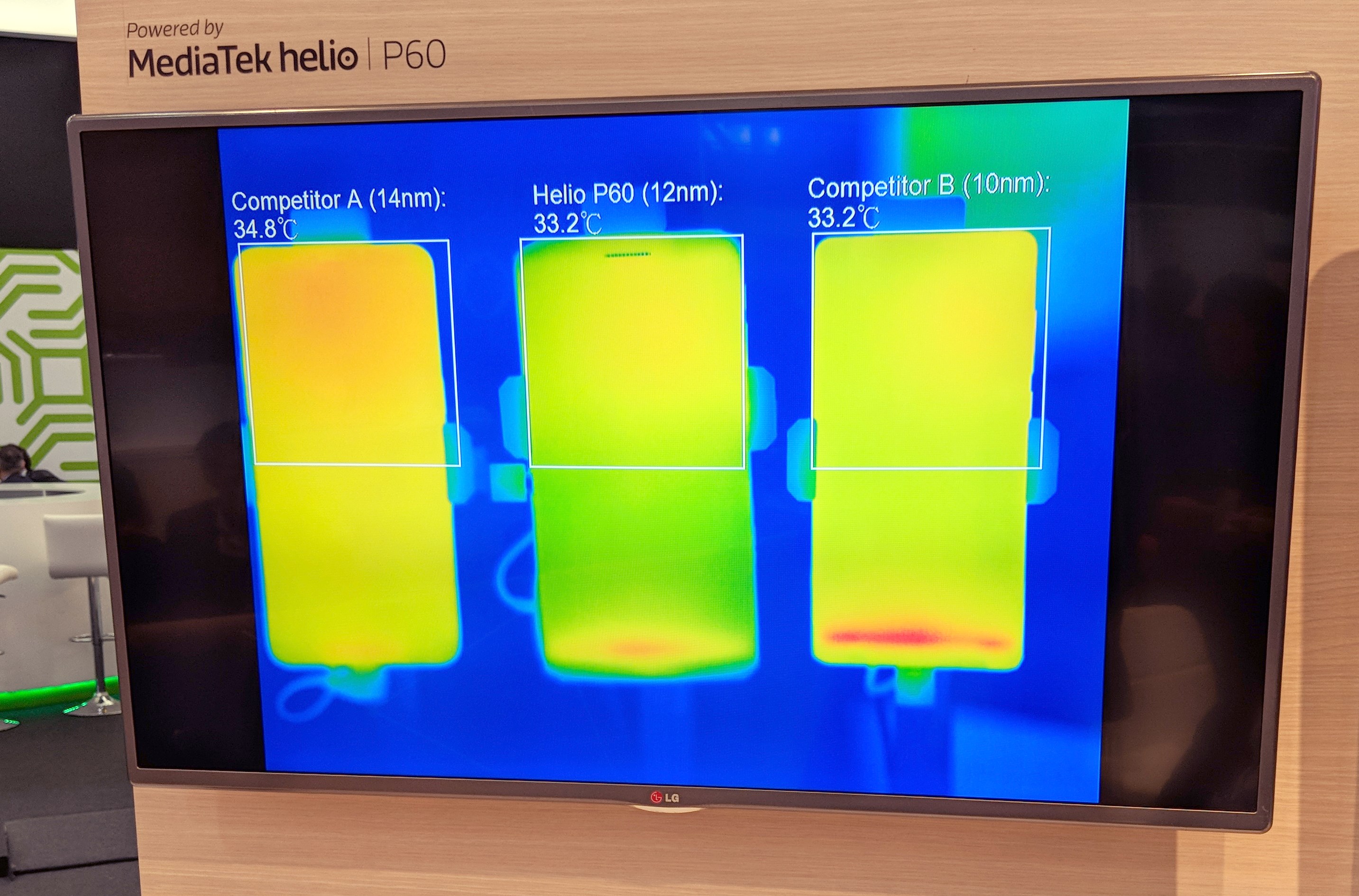
Snapdragon 660 vs Helio P60 vs Snapdragon 835 Thermal Comparison @ MWC2018
The P60 is the first mobile SoC to come manufactured on TSMC’s new 12nm 12FFC process node. 12FFC is a shrink of 16FFC and uses the same tools – it’s a cost effective alternative to the more expensive 10FF process which requires quad-patterning. While 12FFC does not quite achieve the die size reduction that 10FF would, it’s extremely competitive in terms of power characteristics and reaches near the same efficiency. I asked MediaTek about the company process roadmap plan and they will focus exclusively on 12FFC for 2018 and have no plans for further 10nm silicon. The next generation will jump directly to 7nm in mid 2019 (after other vendors) when mass production will have reached mature and cost-effective levels.
The P60 is the first SoC to bring dedicated neural network accelerators into the mid-range. MediaTek’s denomination for such IP is APU (AI Processing Unit) so that’s yet another term added to the varied basket of abbreviations from different companies. MediaTek wouldn’t disclose the IP provider but say’s it’s a dual-core implementation offering 2x140GMACs. MediaTek will offer a custom software stack called NeuroPilot which will be compatible with Google’s NN API and frameworks such as TensorFlow, TF Lite, Caffe and Caffe2.
The modem subsystem remains the same as on the Helio P30 – it supports LTE up to Category 7 with 3x20MHz CA and 300Mbps download speeds and Category 13 with 2x20MHz CA for up to 150Mbps upload speeds.
The Helio P60 is in production now and we should see consumer smartphones with the chipset available starting early Q2 2018.


74 Comments
View All Comments
jjj - Monday, March 5, 2018 - link
@Wardrive86If you got cost, perf and power, for each product there is a choice to be made. Pushing clocks ,leads to higher perf per mm2 and you get payed for that perf. Pretty much any high end SoC is that, in both PC and phones, you always get the highest perf and best perf per cost ratio when you sacrifice efficiency. That can also be done in other segments, not only in high end. Some phone SoCs do that even bellow high end, from a bunch of folks, Qualcomm, Mediatek, Hisilicon.
I did not say that SD845 is terrible just that i suspect it has a minor issue.Other than that , it's pretty good, vs most of Qualcomm's high end SoCs in recent years. The price is terrible but that's because there is no competition and there is no competition because the market is small while costs and risks are high so , if Mediatek does not spend on that, there is nobody else to.
Then the claim that Qualcomm is better is false and so is the "cheap" claim. Mediatek is not cheaper and OEMs do not chose them on price.As noted before, Qualcomm leverages licensing to gain and retain share, on merit ,they would have a lot lower share.
One more little bit that you should consider, in low end, battery costs are very important, a less efficient SoC increases battery costs by too much and in that segment, low power is very important. In high end, the battery's mechanical volume is an issue and it's getting much worse with full screen, foldable displays and 5G- with 5G the antennas are a bit problematic with mmWave.
I understand that folks around here have seen things like the Helio X10 that sacrifice efficiency for cost and perf but you shouldn't generalize. Even Helio X20, that one was on 20nm and 20nm was a nightmare (look at SD810) but aside from that, it was just 100mm2 and sold at some 20$ Clocks were pushed to 2.1GHz because OEMs and consumers prioritize perf. The main mistake was the 20nm choice. Same year they had MT6752 vs the the phone melting SD615 and here Qualcomm made the wrong process choice.
ZolaIII - Monday, March 5, 2018 - link
I don't believe neither of them cut dies, those are still small SoC's so from both development time & economic factor would be justifiable but we won't know that part for sure. Sure it's similar design (so similar that they don't preroote most of it) but I think quartz oscillators & power rails are different.serendip - Monday, March 5, 2018 - link
Zola is right, Qualcomm is pushing clocks too high on the SD845 just to hit nice benchmark figures. That thing will burn power and throttle like a bad joke though. The beauty of the 625 and to a lesser extent, the 650, is that they don't throttle much while still getting decent performance. Hopefully Mediatek gets smart and tries the same approach instead of chasing benchmarks and adding cores just for marketing points. Then again, who am I kidding... Idiot consumers still buy phones based on core counts without bothering about real world performance.ZolaIII - Monday, March 5, 2018 - link
S625 doesn't throttle at all, it's even peak power consumption (it's about 2.1W) doesn't reach 2.5W which is max sustainable. S650 does throttle but not much max sustainable for big A72's is 1.4 GHz (both running) and 450~533 MHz for GPU. Tho in the real use including & extensive gaming S650 rarely fails down to those values. The big cores are 1.8x faster (A72's, A73's) clock per clock in integer performance compared to smaller in order ones & most of the tasks are still integer one's. A75's In comparison to the A55's extend that gap to 2.2x.