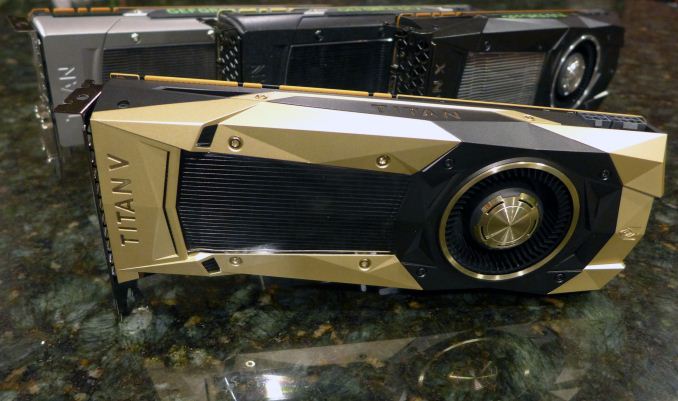
The NVIDIA Titan V Preview - Titanomachy: War of the Titans
by Ryan Smith & Nate Oh on December 20, 2017 11:30 AM EST
Over the years we at AnandTech have had the interesting experience of covering NVIDIA’s hard-earned but none the less not quite expected meteoric rise under the banner of GPU computing. Nearly a decade ago CEO Jen-Hsun Huang put the company on a course to invest heavily in GPUs as compute accelerators, and while it seemed likely to pay off – the computing industry has a long history of accelerators – when, where, and how ended up being a lot different than Huang was first expecting. Instead of the traditional high performance computing market, the flashpoint for NVIDIA’s rapid growth has been in neural networking, a field that wasn’t even on the radar 10 years ago.
I bring this up because in terms of NVIDIA’s product line, I don’t think there’s a card that better reflects NVIDIA’s achievements and shifts in compute strategy than the Titan family. Though originally rooted as a sort of flagship card of the GeForce family that lived a dual life between graphics and compute, the original GTX Titan and its descendants have instead transitioned over the years into an increasingly compute-centric product. Long having lost its GeForce branding but not the graphical capabilities, the Titan has instead drifted towards becoming a high performance workstation-class compute card. Each generation of the Titan has pushed farther and farther towards compute, and if we’re charting the evolution of the Titan, then NVIDIA’s latest Titan, the NVIDIA Titan V, may very well be its biggest jump yet.
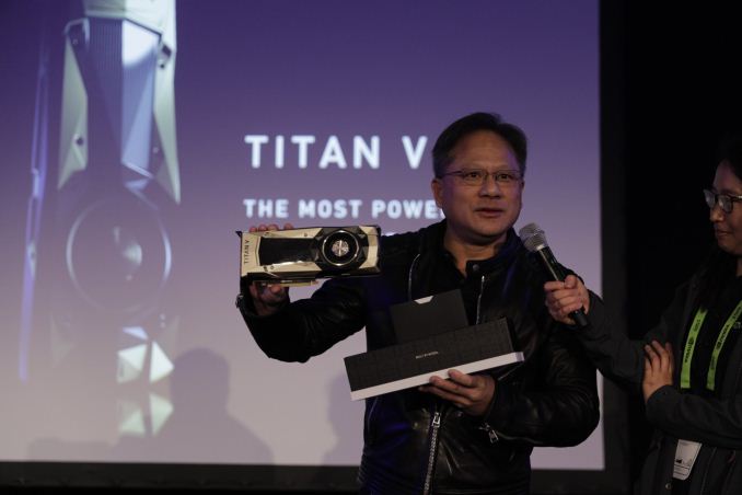
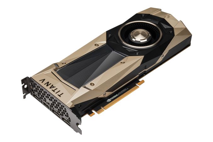
Launched rather unexpectedly just two weeks ago at the 2017 Neural Information Processing Systems conference, the NVIDIA Titan V may be the most important Titan yet for the company. Not just because it’s the newest, or because it’s the fastest – and oh man, is it fast – or even because of the eye-popping $3000 price tag, but because it’s the first card in a new era for the Titan family. What sets the Titan V apart from all of its predecessors is that it marks the first time that NVIDIA has brought one of their modern, high-end compute-centric GPUs to the Titan family, and what that means for developers and users alike. NVIDIA’s massive GV100 GPU, already at the heart of the server-focused Tesla V100, introduced the company’s Volta architecture, and with it some rather significant changes and additions to NVIDIA’s compute capabilities, particularly the new tensor core. And now those features are making their way down into the workstation-class (and aptly named) Titan V.
| NVIDIA GPU Specification Comparison | ||||||
| Titan V | Titan Xp | GTX Titan X (Maxwell) | GTX Titan | |||
| CUDA Cores | 5120 | 3840 | 3072 | 2688 | ||
| Tensor Cores | 640 | N/A | N/A | N/A | ||
| ROPs | 96 | 96 | 96 | 48 | ||
| Core Clock | 1200MHz | 1485MHz | 1000MHz | 837MHz | ||
| Boost Clock | 1455MHz | 1582MHz | 1075MHz | 876MHz | ||
| Memory Clock | 1.7Gbps HBM2 | 11.4Gbps GDDR5X | 7Gbps GDDR5 | 6Gbps GDDR5 | ||
| Memory Bus Width | 3072-bit | 384-bit | 384-bit | 384-bit | ||
| Memory Bandwidth | 653GB/sec | 547GB/sec | 336GB/sec | 228GB/sec | ||
| VRAM | 12GB | 12GB | 12GB | 6GB | ||
| L2 Cache | 4.5MB | 3MB | 3MB | 1.5MB | ||
| Single Precision | 13.8 TFLOPS | 12.1 TFLOPS | 6.6 TFLOPS | 4.7 TFLOPS | ||
| Double Precision | 6.9 TFLOPS (1/2 rate) |
0.38 TFLOPS (1/32 rate) |
0.2 TFLOPS (1/32 rate) |
1.5 TFLOPS (1/3 rate) |
||
| Half Precision | 27.6 TFLOPS (2x rate) |
0.19 TFLOPs (1/64 rate) |
N/A | N/A | ||
| Tensor Performance (Deep Learning) |
110 TFLOPS | N/A | N/A | N/A | ||
| GPU | GV100 (815mm2) |
GP102 (471mm2) |
GM200 (601mm2) |
GK110 (561mm2) |
||
| Transistor Count | 21.1B | 12B | 8B | 7.1B | ||
| TDP | 250W | 250W | 250W | 250W | ||
| Manufacturing Process | TSMC 12nm FFN | TSMC 16nm FinFET | TSMC 28nm | TSMC 28nm | ||
| Architecture | Volta | Pascal | Maxwell 2 | Kepler | ||
| Launch Date | 12/07/2017 | 04/07/2017 | 08/02/2016 | 02/21/13 | ||
| Price | $2999 | $1299 | $999 | $999 | ||
Our traditional specification sheet somewhat understates the differences between the Volta architecture GV100 and its predecessors. The Volta architecture itself sports a number of differences from Pascal, some of which we’re just now starting to understand. But the takeaway from all of this is that the Titan V is fast. Tap into its new tensor cores, and it gets a whole lot faster; we’ve measured the card doing nearly 100 TFLOPs. The GV100 GPU was designed to be a compute monster – and at an eye-popping 815mm2, it’s an outright monstrous slab of silicon – making it bigger and faster than any NVIDIA GPU before it.
That GV100 is appearing in a Titan card is extremely notable, and it’s critical to understanding NVIDIA’s positioning and ambitions with the Titan V. NVIDIA’s previous high-end GPU, the Pascal-based GP100, never made it to a Titan card. That role was instead filled by the much more straightforward and consumer-focused GP102 GPU, leading to the resulting Titan Xp. Titan Xp itself was no slouch in compute or graphics, however it left a sizable gap in performance and capabilities between it and the Tesla family of server cards. By putting GV100 into a Titan card, NVIDIA has eliminated this gap. However it also changes the market for the card and its expectations.
The Titan family has already been pushing towards compute for the past few years, and by putting the compute-centric GV100 into the card, NVIDIA has essentially ushered that transition to completion. The Titan V now gets all of the compute capabilities of NVIDIA’s best GPU, but in turn it’s more distant than ever from the graphics world. Which is not to say that it can’t do graphics – as we’ll see in detail in a bit – but this is first and foremost a compute card. In particular it is a means for NVIDIA to seed development for the Volta architecture and its new tensor cores, and to give its user base a cheaper workstation-class alternative for smaller-scale compute projects. The Titan family may have started as a card for prosumers, but the latest Titan V is more professional than any card before.
Putting this into context of what it means for existing Titan customers, and it means different things for compute and graphics customers. Compute customers will be delighted at the performance and the Volta architecture’s new features; though they may be less delighted at the much higher price tag.
Gamers on the other hand are in an interesting bind. Make no mistake, the Titan V is NVIDIA’s fastest gaming card to date, but as we’re going to see in our benchmarks, at least right now it’s not radically ahead of cards like the GeForce GTX 1080 and its Titan Xp equivalent. As a result, you can absolutely game on the card and boutique system builders are even selling gaming systems with the cards. But as we’re going to see in our performance results, the performance gains are erratic and there are a number of driver bugs that need squashed. The end result is that the messaging from NVIDIA and its partners is somewhat inconsistent; the $3000 price tag and GV100 GPU scream compute, but then there’s the fact that it does have video outputs, uses the GeForce driver stay, and is NVIDIA’s fastest GPU to date. I expect interesting things once we have proper consumer-focused Volta GPUs from NVIDIA, but that is a proposition or next year.
Getting down to the business end of things, let’s talk about today’s preview. In Greek mythology Titanomachy was the war of the Titans, and for our first look at the Titan V we’re staging our own version of Titanomachy. We’ve rounded up all four of the major Titans, from the OG GTX Titan to the new Titan V, and have tested them on a cross-section of compute, gaming, and professional visualization tasks in order to see what makes the Titan V tick and how the first graphics-enabled Volta card fares. Today’s preview is just that, a preview – we have even more benchmarks cooking in the background, including some cool deep learning stuff that didn’t make the cut for today’s article. But for now we have enough data pulled together to see how NVIDIA’s newest Titan compares to its siblings, and why the Volta architecture just may be every bit as big of a deal as NVIDIA has been making of it.


111 Comments
View All Comments
mode_13h - Wednesday, December 27, 2017 - link
It's true. All they had to do was pay some grad students to optimize HPC and deep learning software for their GPUs. They could've done that for the price of only a couple marketing persons' salaries.CiccioB - Monday, January 1, 2018 - link
That would not be a surprise.AMD strategy on SW support has always been leaving others (usually not professionist) do the job at their own cost. Results is that AMD HW has never had a decent SW support other than for gaming (and that's only because Sony and MS spend money for improving gaming performances for their consoles).
tipoo - Friday, December 22, 2017 - link
Sarcasm? There's no Vega built up to this scale.mode_13h - Wednesday, December 27, 2017 - link
It *is* pretty big and burns about as much power. Yet, it's nowhere near as fast at deep learning. Even with its lower purchase price, it's still not operationally cost-competitive with GV100.If you look at its feature set, it was really aimed at HPC and deep learning. In the face of Volta's tensor cores, it kinda fell flat, on the latter front.
Keermalec - Wednesday, December 20, 2017 - link
What about mining benchmarks?tipoo - Friday, December 22, 2017 - link
Would be in line with the CUDA improvements. I.e, two 1080s would be much better at mining. Most of the uplift is in tensor performance, which no algo uses.Cryio - Wednesday, December 20, 2017 - link
Wait wait wait.Crysis Warhead at 4K, Very High with 4 times Supersampling? I think you mean Multisampling.
I don't think this could manage 4K60 at max settings with 4xSSAA, lol.
Ryan Smith - Thursday, December 21, 2017 - link
"I think you mean Multisampling."Nope, supersampling.=)
mode_13h - Wednesday, December 27, 2017 - link
Tile rendering FTMFW.Kevin G - Wednesday, December 20, 2017 - link
"For our full review hopefully we can track down a Quadro GP100"YES. The oddity here is that the GP100 might end up being better than the Titan V at gaming due to having 128 ROPs vs. 96 ROPs and even higher memory bandwidth.
Outside of half precision matrix multiplication, the GP100 should be roughly ~43% faster due mainly to the difference in ALU counts in professional workloads. Boost clocks are a meager 25 Mhz difference. Major deviations beyond that 43% difference would be where the architectures differ. There is a chance benchmarks would come in below that 43% mark if memory bandwidth comes into play.