Qualcomm Announces Snapdragon 845 Mobile Platform: Tocks Next-Gen CPU Cores, GPU, AI, & More
by Andrei Frumusanu on December 6, 2017 5:30 PM EST- Posted in
- Mobile
- Snapdragon
- Qualcomm
- Smartphones
- SoCs
- 10nm
- Snapdragon 845

Today as part of its media event, Qualcomm finally announced the much expected Snapdragon 845, successor to last year's very successful Snapdragon 835. The Snapdragon 845 is a large step in terms of SoC architectures as it's the first to employ ARM's DynamiQ CPU cluster organization. Quickly explained, DynamIQ enables the various different CPU cores within an SoC to be hosted within the same cluster and cache hierarchy, as opposed to having separate discrete clusters with no shared cache between them (with coherency instead happening over an interconnect such as ARM's CCI). This major transition is probably the largest to date that we've seen in modern mobile smartphone ARM consumer SoCs.
| Qualcomm Snapdragon Flagship SoCs 2017-2018 | |||
| SoC | Snapdragon 845 | Snapdragon 835 | |
| CPU | 4x Kryo 385 Gold (A75 derivative) @ 2.8GHz 4x256KB L2 4x Kryo 385 Silver (A55 derivative) @ 1.80GHz 4x128KB L2 2MB L3 |
4x Kryo 280 Gold (A73 derivative) @ 2.45GHz 2MB L2 4x Kryo 280 Silver (A53 derivative) @ 1.90GHz 1MB L2 |
|
| GPU | Adreno 630 | Adreno 540 @ 670/710MHz | |
| Memory | 4x 16-bit CH @ 1866MHz LPDDR4x 29.9GB/s 3MB system cache |
4x 16-bit CH @ 1866MHz LPDDR4x 29.9GB/s |
|
| ISP/Camera | Dual 14-bit Spectra 280 ISP 1x 32MP or 2x 16MP |
Dual 14-bit Spectra 180 ISP 1x 32MP or 2x 16MP |
|
| Encode/ Decode |
2160p60 10-bit H.265 720p480 |
2160p30 (2160p60 decode), 1080p120 H.264 & H.265 |
|
| Integrated Modem | Snapdragon X20 LTE (Category 18/13) DL = 1200Mbps 5x20MHz CA, 256-QAM UL = 150Mbps 2x20MHz CA, 64-QAM |
Snapdragon X16 LTE (Category 16/13) DL = 1000Mbps 3x20MHz CA, 256-QAM UL = 150Mbps 2x20MHz CA, 64-QAM |
|
| Mfc. Process | 10nm LPP | 10nm LPE | |
The CPU
The Snapdragon 835's Kryo 280 performance and efficiency cores make use of ARM's Built on ARM Cortex Technology license which allows Qualcomm to make requests to ARM to change some aspects of the architectures of newly released cores and implement these changes exclusively into Snapdragon SoCs. As such the S835's CPU cores were derivatives of ARM's Cortex A73 and Cortex A53 CPU IPs. The Snapdragon 845 being the first SoC to be based on a DynamIQ big.LITTLE CPU organization also undoubtedly suggests that the Kryo 385 CPUs are based on ARM's Cortex A75 and Cortex A55 IPs, as these are the only DynamIQ compatible CPU cores available to date.
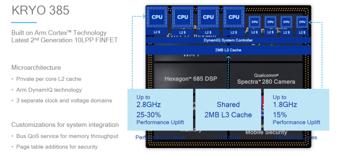
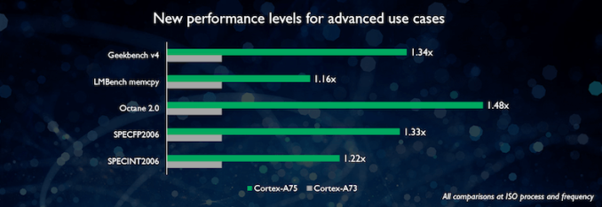
The Kryo 385 gold/performance cluster runs at up to 2.8GHz, which is a 14% frequency increase over the 2.45GHz of the Snapdragon 835's CPU core. But we also have to remember that given that the new CPU cores are likely based on A75's we should be expecting IPC gains of up to 22-34% based on use-cases, bringing the overall expected performance improvement to 39-52%. Qualcomm promises a 25-30% increase which is at the low-end of ARM's projections.
The silver/efficiency cluster is running at 1.8GHz, this is clocked slightly slower than the A53's on the Snapdragon 835 however the maximum clocks of the efficiency cluster is mainly determined by where the efficiency curve of the performance cluster intersects. Nevertheless the efficiency cores promise 15% boost in performance compared to its predecessor.
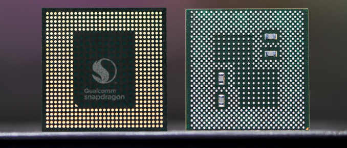
The new Snapdragon 845 now includes capacitors on its package underside
The L3 located on the DynamIQ DSU is configured at 2MB and we're likely seeing 256KB/128KB options for the performance and efficiency core private L2's. Together this would mean there's a total of 3.5MB of combined L2 and L3 cache on the CPU complex.
Qualcomm interestingly disclosed that we're only seeing three voltage and frequency planes implemented; likely meaning a single plane each for the performance cores as well as the efficiency cores as well as a plane for the L3 and DSU. This is surprising as DynamIQ allows finer grained frequency/voltage planes and given Qualcomm being traditionally a big proponent of asymmetric planes such as implemented in Krait I would have expected to see a more non-traditional approach, something that would have been facilitated given the fact that Qualcomm likes to include on-chip LDO regulators for powering the CPU clusters.
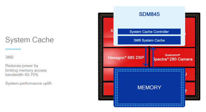
Related to the caches but not part of the CPU, there's also a new inclusion of a 3MB system cache. This is likely a SoC interconnect cache and serves all SoC blocks - likely in similar fashion the "L3" cache on Apple A-series SoCs works. This would help reduce external memory transactions and thus also reduce power to the memory controllers and DRAM. Qualcomm claims it's able to reduce memory access bandwidth by up to 40-75%, a significant figure.
The GPU
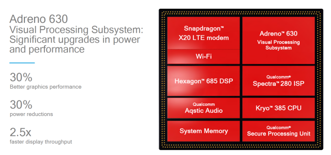
The Snapdragon 845 comes with a new generation of the Adreno GPU, called the Adreno 630. The switch from a 5xx family to a 6xx family GPU, as with previous introductions from Qualcomm usually marks the transition consisting of larger architectural changes.
Qualcomm is as usual very tight-lipped about details of its GPU but it promises a performance increase of 30% while also increasing power-efficiency by 30%. What this translates to is basically we're looking at 30% higher frame-rates while maintaining the same power consumption of the Snapdragon 835, which is an excellent improvement.
DSP Upgrade to Hexagon 685
The DSP sees a evolutionary upgrade from the 682 to the 685. Again details about the improvements are relatively sparse but Qualcomm promises improvements in power and performance, especially for AI and imaging tasks. Qualcomm made an emphasis on AI processing during the presentation and claim that the new IP achieves up to 3x increase in performance compared to the Snapdragon 835.
Traditional DSP architectures are usually not well optimized for neural network processing so we'll have to adopt a wait & see approach when it comes to the performance of the new Hexagon 685 when executing such tasks. SoCs which have a dedicated NPU such as the Apple A11 or Kirin 970 still have a large edge here as they augment the image processing pipeline instead of handing such tasks over to the DSP which might have to do double duty of both image processing (such as HDR) and image analysis via neural network processing (image recognition and classification).
Snapdragon X20 Modem Now Integrated
As is traditional with Qualcomm we first see cutting-edge modem implementations first released as independent discrete modems and only afterwards do we see them integrated into the newest high-end SoCs. The Snapdragon 845 now integrated the X20 modem released earlier in the year which we've covered in a dedicated article.
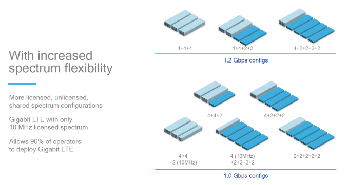
The new modem elevates the LTE UE Category to 18 as it's now capable of 5xCA as opposed to 4xCA on the X16 modem integrated in the Snapdragon 835. This allows for download speeds of up to 1.2Gbps when in a 5x20MHz downstream carrier aggregation mode, that is of course, if you're lucky enough for your mobile carrier to support such configurations.
Improved Media Capabilities
The Snapdragon 845's display pipeline receives an upgrade for VR and claims to be now able to drive dual-2400x2400p120 displays for VR headsets. The video recording capabilities have been improved as the Snapdragon 845 increases maximum video encoding framerate at 4K recording from 30 to 60fps compared to the Snapdragon 835. Qualcomm advertised support for Rec.2020 wide gamut color space recording, meaning we now see full support for HDR10 HEVC recording which should be an interesting addition I'm looking forward to test.
The new Spectra 280 ISP's most standout feature seems to be multi frame noise reduction (MFNR) which is a feature that I believe is also used in Google's HDR+ proprietary processing. The feature captures multiple pictures in fast succession and applies an algorithm to apply noise reduction in higher quality fashion compared to traditional single-frame noise reduction which can introduce blurriness.
Manufactured on Second Generation 10LPP Process
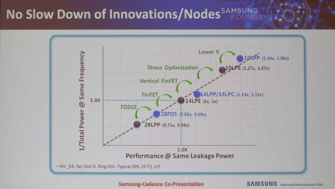
The Snapdragon 845 comes manufactured on a second generation 10LPP process from Samsung. This was a natural evolution to be expected as the Snapdragon 835 was manufactured on 10LPE. Samsung promises performance increase of up to 10% at the same power levels or reduced power consumption of up to 15% at the same performance. Samsung had just announced last week the start of mass production for 10LPP. I was rather surprised to see the larger frequency boost to 2.8GHz on the performance cores as the Snapdragon 835 came with rather conservative frequencies of only 2.45. The A75 promised increased performance at the same efficiency, meaning the core uses more power to reach the higher performance point compared to the A73.
Most devices I've seen with Snapdragon 835's used about 1.1W per core at peak using the power virus-style workload we traditionally use so seeing the Snapdragon 845 using the new processor architecture as well as increases in frequency is quite surprising as both would increase the absolute power consumption of the CPUs. The two possible scenarios we're likely to encounter is that either the Snapdragon 845 CPU complex uses more power or that Samsung has managed to vastly improve its manufacturing process over the last year to allow for such gains.
"Tock" Generation For CPU and GPU
The new Snapdragon 845 brings with itself one of the biggest architectural shifts in the ARM SoC space with the first implementation of the new DynamIQ cluster hierarchy. With an expected solid 30% performance boost on both CPU and GPU we're likely to see a healthy upgrade for 2018 flagship devices. Overall the Snapdragon 845 fulfils most of its expectations and in a time in the Android ecosystem where improvements have slowed down this is a good thing. The Snapdragon 835 was an excellent SoC as it balanced performance and power perfectly and thus re-solidified Qualcomm's positioning as the go-to solution for mobile SoCs. On paper the Snapdragon 845 seems to continue this balance and if all goes as planned we're likely to see another healthy generation of devices in 2018 that we're eagerly awaiting to review.




145 Comments
View All Comments
Arbie - Thursday, December 7, 2017 - link
@generalako - Where do you get off being abusive? Go start flame wars somewhere else. This was a decent read until I hit your post. No call for it.jwcalla - Wednesday, December 6, 2017 - link
You'd have to run Android on both the Apple chip and Qualcomm chip to get an accurate benchmark.Compiler differences alone can explain benchmark differences.
SquarePeg - Wednesday, December 6, 2017 - link
Yes people often point out Geekbench but it's actually worthless when comparing different hardware on different software platforms. The only thing Geekbench is remotely accurate at is comparing hardware evolution's on the same software platforms such as A9 to A10 or SD 835 to SD 845. You only have to dual boot Windows and Linux on a desktop and run Geekbench 4 on both to see how massively different it's results are from OS to OS. But you have a fair number of mindless people who think an iPhone is as powerful as a Macbook Pro because of Geekbench's useless cross-platform results.Quantumz0d - Wednesday, December 6, 2017 - link
Second this.Always people compare these Apples to Oranges. Plus people also forget how the SD82x platform broke the A9 to shreds.
This is again a semi-custom chip we are looking at same like the 835 instead of a full custom like Kyro or Krait. Also the A series chips are very expensive thus the higher price and Apple has more R&D expenditure in that regard. Not that Qcomm cannot but bleeding that much cash into that ecosystem will break their bank, given the NXP case, Apple lawsuits across the world, Patent game and the market footing.
Also the Qcomm SD platform has undisputed advantage when it comes to OSS development, No other SoC can compete with them, Exynos Pre SIII used to but Samsung chose different path, Maybe Kirin but it's not transparent or ahead of the league with CAF like Qcomm.
BillBear - Thursday, December 7, 2017 - link
Ummm, no.The current version of Geekbench uses big ass chunks of commonly used open source code compiled for each platform and running the exact same workload.
For instance, one of the tests is to use PDF rendering code from the Chrome web browser to render the same PDF on each platform.
It tests things like LLVM compiling source code, SQLight running database tests, the LUA scripting language used in so many games, Chrome rendering HTML and PDF, etc.
https://www.geekbench.com/doc/geekbench4-cpu-workl...
tuxRoller - Thursday, December 7, 2017 - link
Maybe my reading skills are slipping but that doc is extremely high level with no links to their repo or even compiler settings (oh yeah, they use different compilers for different platforms, so, that's not great).HStewart - Thursday, December 7, 2017 - link
I would agree on this - Geekbench is not a reliable benchmark. I seriously don't believe we have good set of benchmarks - to actually to explain the differences of cpu's especially between x86 and ARM processors.For one thing there is a big difference between RISC (ARM) and CISC (x86) architectures. By designed CISC has complex instruction - meaning that it instructions can handle more complex instructions on execution. This has even got more complex with instruction extension AVX2 and now AVX 512
RISC on the other hand is Reduce Instruction Set - this means it has simpler instruction, which can be process more efficiently. This means for complex activity it takes more instructions to handle the instruction.
I used to be very heavy into CPU architecture as OS developer and at Georgia Tech, I had class on Micro Code program - but CISC and RISC eventually get coded down into Microcode. I have heard that Intel has change the designed of Microcode to take away the advantage of RISC instruction in the instruction pipeline - by change the way the instruction work on pipeline.
Most interesting things that I heard in this area - is propose technical rumors of 10nm - which is about optimized MOVS instructions - this is extremely frequent code that compilers and also people that hand assembly instructions ( pretty rare now )
There is a book called "80x86 Architexture & Programing" by Rakesh K. Agarwal" 1991 which can pretty much provide pseudo code for each of x86 instructions at the time. If the rumors are correct Qualcomm made some optimizations for x86 - I could see them creating new instructions to make it run fasters - books like this one and others knowledge could help.
Then it proposes a bigger question, does the Qualcomm process become ARM processor with Intel x86 emulation - is it going to be another Intel clone cpu like AMD CPU.
As for as "iPhone is as powerful as a Macbook Pro because of Geekbench's useless cross-platform results.", this could be true in my case of hardware. iPhone 6 and MacBook Pro 13 in 2009 with Core 2 Duo 2.2Ghz. There is no way even iPhone X is anything close to new MacBook Pro in real life.
Wilco1 - Thursday, December 7, 2017 - link
I would suggest you read some more books and do some actual programming before making many obviously false claims. The Hennessy&Patterson book is biased towards MIPS but OK for beginners learning about RISC and CISC. https://www.amazon.co.uk/Computer-Architecture-Qua...The fact is Arm and AArch64 typically require fewer instructions than x86. This is simply about good ISA design: adding only instructions which are useful to compilers. It's funny you mention REP MOVSB, that's a perfect example of a complex and slow instruction that is never used by compilers. This has been the case for the last 30 years - even in the latest x86 CPUs, REP MOVSB is something like 3x slower than a hand coded memcpy for typical sizes...
HStewart - Thursday, December 7, 2017 - link
"It's funny you mention REP MOVSB, that's a perfect example of a complex and slow instruction that is never used by compilers"It is obvious some people have no idea of compiles - at least for C++ a lot of times when moving variables around translated from C++ code to actual assembly code
I compile a simple MFC apps and found tons of Rep MOv instructions
_this$ = ecx
push ebp
mov ebp, esp
sub esp, 204 ; 000000ccH
push ebx
push esi
push edi
push ecx
lea edi, DWORD PTR [ebp-204]
mov ecx, 51 ; 00000033H
mov eax, -858993460 ; ccccccccH
rep stosd
"This has been the case for the last 30 years - even in the latest x86 CPUs, REP MOVSB is something like 3x slower than a hand coded memcpy for typical sizes..."
do you realize that memcpy actually is c function that actually used REPSV to implement. Don't just take my word take people who discuss internals of Linux kernel.
https://stackoverflow.com/questions/27705053/memcp...
"The Hennessy&Patterson book is biased towards MIPS but OK for beginners learning about RISC and CISC. https://www.amazon.co.uk/Computer-Architecture-Qua...
This books looks like actually a new of version of book I had at Georgia Tech in 1980's - yes things have change - but I have over 30 years in software development including almost seven years in Intel assembly Operating System development - including finding erratum in CPU related to 386 Protected mode code.
"The fact is Arm and AArch64 typically require fewer instructions than x86"
You do realize by nature of CISC by it nature a single CISC takes many RISC instruction to execute.
HStewart - Thursday, December 7, 2017 - link
Actual my example above has rep stosb - but it very similar to rep mov - which as mention above is all C "memcpy" command is implemented.Sorry about this - but unless I have not found this site does allow edits.