Samsung Increases Production Volumes of 8 GB HBM2 Chips Due to Growing Demand
by Anton Shilov on July 19, 2017 8:00 AM EST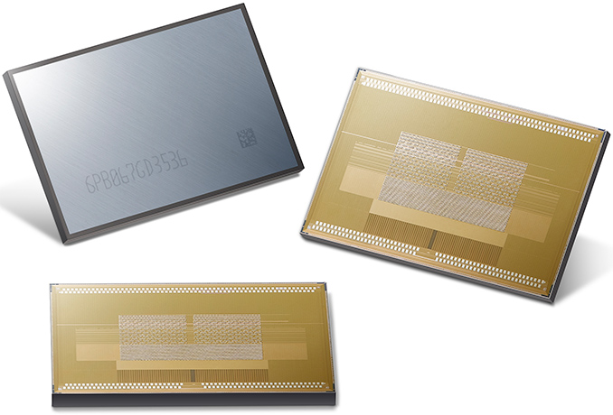
Samsung on Tuesday announced that it is increasing production volumes of its 8 GB, 8-Hi HBM2 DRAM stacks due to growing demand. In the coming months the company’s 8 GB HBM2 chips will be used for several applications, including those for consumers, professionals, AI, as well as for parallel computing. Meanwhile, AMD’s Radeon Vega graphics cards for professionals and gamers will likely be the largest consumers of HBM2 in terms of volume. And while AMD is traditionally a SK Hynix customer, the timing of this announcement with AMD's launches certainly suggests that AMD is likely a Samsung customer this round as well.
Samsung’s 8 GB HBM Gen 2 memory KGSDs (known good stacked die) are based on eight 8-Gb DRAM devices in an 8-Hi stack configuration. The memory components are interconnected using TSVs and feature over 5,000 TSV interconnects each. Every KGSD has a 1024-bit bus and offers up to 2 Gbps data rate per pin, thus providing up to 256 GB/s of memory bandwidth per single 8-Hi stack. The company did not disclose power consumption and heat dissipation of its HBM memory components.
Update 7/20: Samsung confirmed that the DRAM devices are made using 20 nm process technology, but could not disclose power consumption and TDP of KGSDs.
Samsung began mass production of 4-Hi HBM2 KGSDs with 4 GB capacity and 2 Gbps data rate per pin in early 2016. These chips have been used to build various solutions based on NVIDIA’s GP100 and later GV100 GPUs aimed at HPC and similar applications. The company also started to manufacture HBM2 KGSDs with 8 GB capacity in 2016 and so far, Samsung is the only company to publicly announce that they can mass-produce 8 GB HBM2 KGSDs.

Recently AMD launched its Radeon Vega Frontier Edition cards, the first commercial products featuring Vega and 8-Hi HBM2 stacks. To date we haven't been able to get confirmation of whose HBM2 AMD is using – frequent collaborator SK Hynix's or Samsung’s – however as Samsung is for now the only vendor to announce 8-Hi volume production, it's looking increasingly likely that AMD is using Samsung's HBM2. Meanwhile in the coming months AMD will expand the lineup of its graphics cards based on the Vega GPU with the RX Vega line for gamers, and considering that such devices are sold in mass quantities, Samsung has a very good reason for increasing HBM2 production..
Samsung expects 8 GB HBM2 KGSDs to account for over 50% of its HBM2 production by the first half of 2018.


Related Reading:
Source: Samsung


33 Comments
View All Comments
DanNeely - Wednesday, July 19, 2017 - link
The one number I'd like to see is power consumption (both the ram chips and the GPUs memory controllers) because the stated reason for HBM over newer additions of GDDR a few years ago was supposed to be power consumed by the IO buses would get out of hand and eat the majority of the TDP budget in the latter case. Since then we've had GDDR5x and GDDR6 which suggests that the GDDR team has managed to do better than was feared at the time.Manch - Wednesday, July 19, 2017 - link
Fr hbm1 anands deep dive it was a good bit. Of power saving. I would like to know the numbers as well.Mainly bc I'd like to throttle back a fury card to see how much of a regression it would beDanNeely - Wednesday, July 19, 2017 - link
I'm 99% sure I saw the deep dive a few years ago. I know what was claimed for power savings then without having to reread the old propaganda. I'm interested in what its actually delivering now, and how the GDDR developers have apparently avoided the power apocalypse that was supposed to ruin them beyond GDDR5.ImSpartacus - Wednesday, July 19, 2017 - link
Yeah, it's a little disappointing, but it's not entirely clear "who" is at fault.Recall that Fiji's HBM was overvolted to 1.3V in order to meet performance requirements. That's going to nullify some power savings.
Similarly, HBM2 doesn't appear to want to clock at 2.0 Gbps (GP100's only went to 1.4 Gbps, GV100 at 1.75 Gbps and the low-volume Vega FE at a weird 1.89 Gbps).
So some of the shortcomings of HBM, itself, appear to nullify its advantages over equivalent GDDR.
But yeah, it hasn't been paired with the best consumer GPUs on the market, so that hurts as well.
Yojimbo - Wednesday, July 19, 2017 - link
The memory manufacturers are at fault. They are the ones who promised and they are the ones who haven't delivered. The fact that NVIDIA put only 16 GB of VRAM on the V100 says a lot. The V100 is a card that is priced at perhaps $13,000 and contains a GPU with a die greater than 800 mm^2. NVIDIA didn't use 16 GB instead of 32 GB because of cost concerns. Apparently the memory manufacturers can't run 8-hi HBM2 stacks at high enough clocks to give the promised bandwidth so NVIDIA had to choose between more capacity or higher bandwidth. Having that extra 16 GB of memory capacity is actually rather important for HPC and AI uses, just not as important as memory bandwidth.I don't know what advantage 8-hi HBM2 has over GDDR5X/6 at this point, other than power usage and PCB area. Those things might be more relevant for networking products that use high bandwidth RAM than for GPUs.
Santoval - Wednesday, July 19, 2017 - link
Navi's design has been most likely locked, and it should currently be at the prototyping stage. Nvidia recently entertained the possibility of developing an MCM (multi-chip-package) GPU, in a similar way to AMD's Threadripper and Epyc, because they say monolithic dies cannot get any bigger (than Volta). It will basically be like a very tightly packed, ultra low latency SLI, and they said the drivers will present the distinct dies as a single one to games and GPU compute apps (and to the OS, of course).It is unknown if they are planning this for the successor of Volta or for generation after that. 7 or 10 nm (for Volta's successor) should allow them to add transistors and shader cores without enlarging the die further, so my guess is that Volta's successor will still be a monolithic die. AMD's potential plans about possible MCM GPUs are also unknown at this point.
extide - Wednesday, July 19, 2017 - link
According to GPU-Z screenshots that I have seen -- (at least some) Vega FE cards run MICRON HBM2, which is definitely surprising as I didn't even know they were in the HB2 game at all, betting solely on GDDR5x/6 -- of course GPU-Z could be wrong, but it is interesting none-the-less.HighTech4US - Wednesday, July 19, 2017 - link
I believe GPU-Z does not actually read the memory data from the actual memory just a copy and paste text string from the program.Ryan Smith - Wednesday, July 19, 2017 - link
Thankfully, GPU-Z gets it very wrong in this case, which makes it clear that it is wrong to being with. Micron doesn't make HBM (they're focused on HMC).Santoval - Wednesday, July 19, 2017 - link
So I guess Vega consumer will use two 4 GB 4-Hi stack KGSDs and Vega semi-pro will use two 8 GB 8-Hi stack KGSDs? These 8-Hi stack chips must still be too expensive.. I wonder how much more a 8 GB 8-Hi chip might cost than two 4 GB 4-Hi ones. I am kind of amazed though that even Tesla GV100 will use 4-Hi stack chips, since this is a part that can certainly swallow the extra cost. Unless Nvidia is worried about the availability of Hi-8 stack chips and/or the design was completed and locked with twice the number of HBM2 chips (compared to a design with 8 GB chips).