AMD Prepares 32-Core Naples CPUs for 1P and 2P Servers: Coming in Q2
by Ian Cutress on March 7, 2017 10:15 AM EST- Posted in
- Enterprise
- CPUs
- AMD
- SoCs
- Enterprise CPUs
- Zen
- Naples
- Ryzen
For users keeping track of AMD’s rollout of its new Zen microarchitecture, stage one was the launch of Ryzen, its new desktop-oriented product line last week. Stage three is the APU launch, focusing mainly on mobile parts. In the middle is stage two, Naples, and arguably the meatier element to AMD’s Zen story.
A lot of fuss has been made about Ryzen and Zen, with AMD’s re-launch back into high-performance x86. If you go by column inches, the consumer-focused Ryzen platform is the one most talked about and many would argue, the most important. In our interview with Dr. Lisa Su, CEO of AMD, the launch of Ryzen was a big hurdle in that journey. However, in the next sentence, Dr. Su lists Naples as another big hurdle, and if you decide to spend some time with one of the regular technology industry analysts, they will tell you that Naples is where AMD’s biggest chunk of the pie is. Enterprise is where the money is.
So while the consumer product line gets columns, the enterprise product line gets profits and high margins. Launching an enterprise product that gains even a few points of market share from the very large blue incumbent can implement billions of dollars to the bottom line, as well as provided some innovation as there are now two big players on the field. One could argue there are three players, if you consider ARM holds a few niche areas, however one of the big barriers to ARM adoption, aside from the lack of a high-performance single-core, is the transition from x86 to ARM instruction sets, requiring a rewrite of code. If AMD can rejoin and a big player in x86 enterprise, it puts a small stop on some of ARMs ambitions and aims to take a big enough chunk into Intel.
With today’s announcement, AMD is setting the scene for its upcoming Naples platform. Naples will not be the official name of the product line, and as we discussed with Dr. Su, Opteron one option being debated internally at AMD as the product name. Nonetheless, Naples builds on Ryzen, using the same core design but implementing it in a big way.
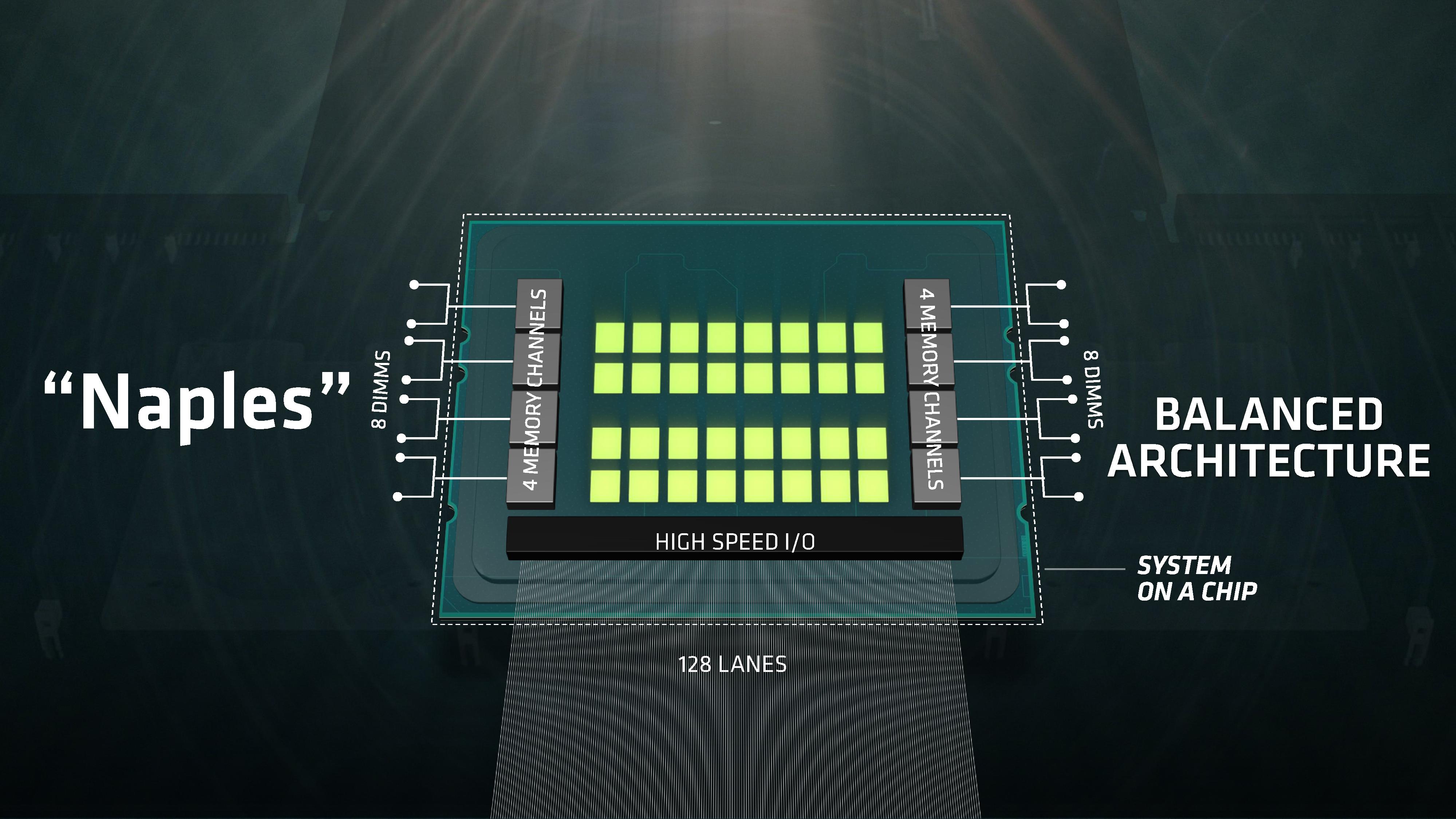
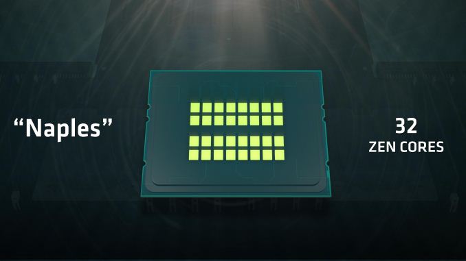
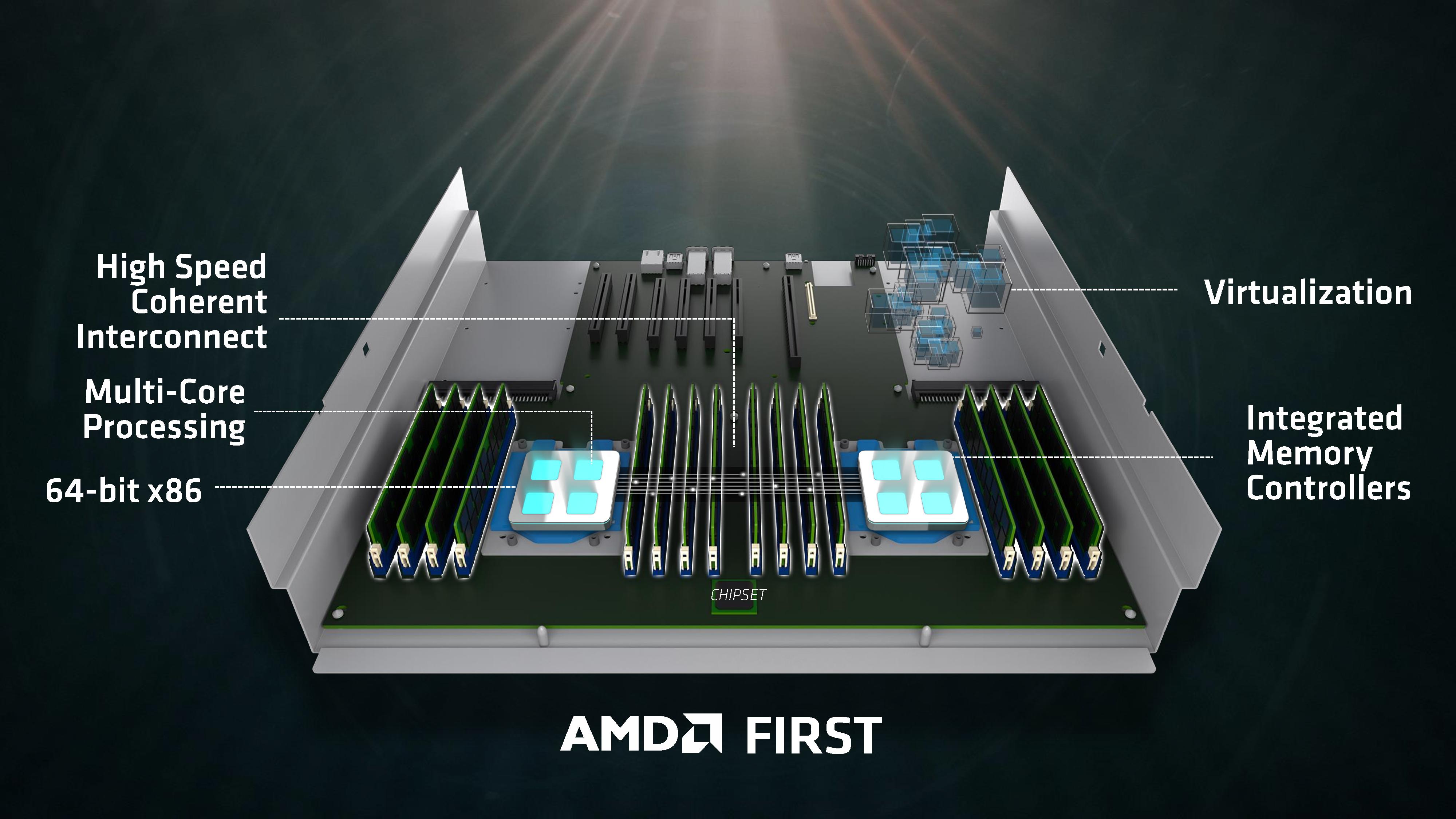
The top end Naples processor will have a total of 32 cores, with simultaneous multi-threading (SMT), to give a total of 64 threads. This will be paired with eight channels of DDR4 memory, up to two DIMMs per channel for a total of 16 DIMMs, and altogether a single CPU will support 128 PCIe 3.0 lanes. Naples also qualifies as a system-on-a-chip (SoC), with a measure of internal IO for storage, USB and other things, and thus may be offered without a chipset.
Naples will be offered as either a single processor platform (1P), or a dual processor platform (2P). In dual processor mode, and thus a system with 64 cores and 128 threads, each processor will use 64 of its PCIe lanes as a communication bus between the processors as part of AMD’s Infinity Fabric. The Infinity Fabric uses a custom protocol over these lanes, but bandwidth is designed to be on the order of PCIe. As each core uses 64 PCIe lanes to talk to the other, this allows each of the CPUs to give 64 lanes to the rest of the system, totaling 128 PCIe 3.0 again.
On the memory side, with eight channels and two DIMMs per channel, AMD is stating that they officially support up to 2TB of DRAM per socket, making 4TB in a single server. The total memory bandwidth available to a single CPU clocks in at 170 GB/s.

While not specifically mentioned in the announcement today, we do know that Naples is not a single monolithic die on the order of 500mm2 or up. Naples uses four of AMD’s Zeppelin dies (the Ryzen dies) in a single package. With each Zeppelin die coming in at 195.2mm2, if it were a monolithic die, that means a total of 780mm2 of silicon, and around 19.2 billion transistors – which is far bigger than anything Global Foundries has ever produced, let alone tried at 14nm. During our interview with Dr. Su, we postulated that multi-die packages would be the way forward on future process nodes given the difficulty of creating these large imposing dies, and the response from Dr. Su indicated that this was a prominent direction to go in.
Each die provides two memory channels, which brings us up to eight channels in total. However, each die only has 16 PCIe 3.0 lanes (24 if you want to count PCH/NVMe), meaning that some form of mux/demux, PCIe switch, or accelerated interface is being used. This could be extra silicon on package, given AMD’s approach of a single die variant of its Zen design to this point.
Note that we’ve seen multi-die packages before in previous products from both AMD and Intel. Despite both companies playing with multi-die or 2.5D technology (AMD with Fury, Intel with EMIB), we are lead to believe that these CPUs are similar to previous multi-chip designs, however there is Infinity Fabric going through them. At what bandwidth, we do not know at this point. It is also pertinent to note that there is a lot of talk going around about the strength of AMD's Infinity Fabric, as well as how threads are manipulated within a silicon die itself, having two core complexes of four cores each. This is something we are investigating on the consumer side, but will likely be very relevant on the enterprise side as well.
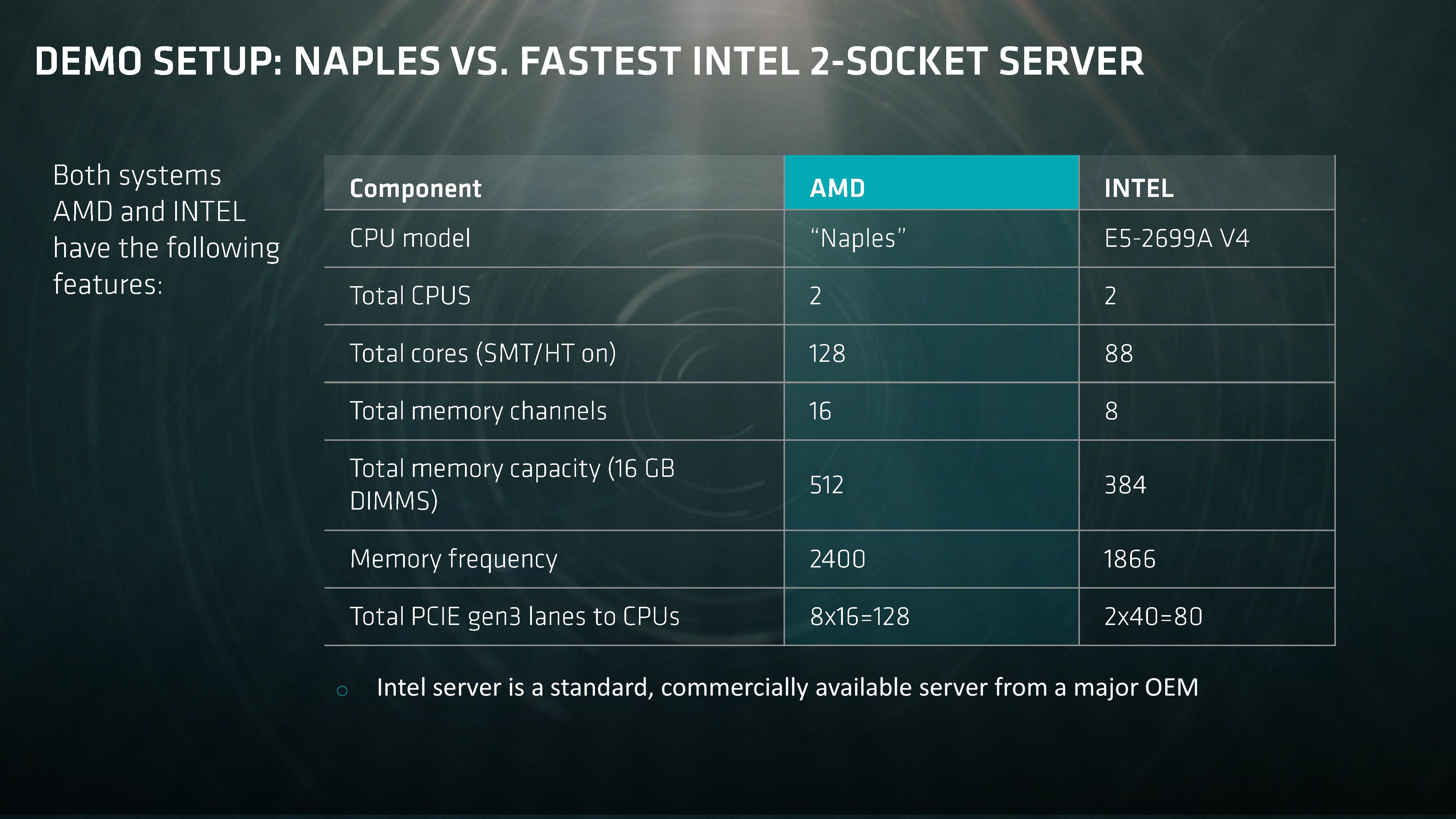
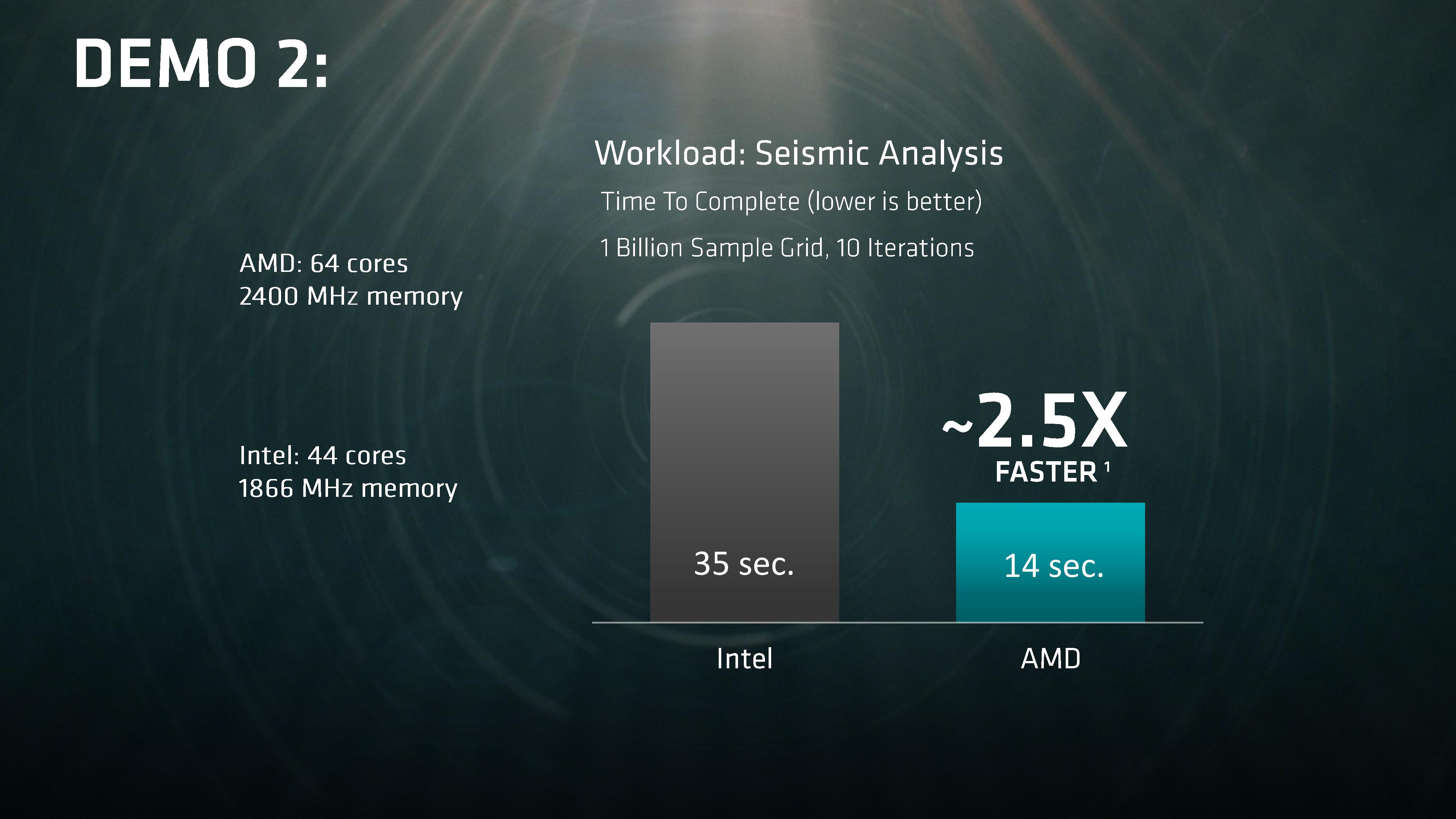
In the land of benchmark numbers we can’t verify (yet), AMD showed demonstrations at the recent Ryzen Tech Day. The main demonstration was a sparse matrix calculation on a 3D-dataset for seismic analysis. In this test, solving a 15-diagonal matrix of 1 billion samples took 35 seconds on an Intel machine vs 18 seconds on an AMD machine (both machines using 44 cores and DDR4-1866). When allowed to use its full 64-cores and DDR4-2400 memory, AMD shaved another four seconds off. Again, we can’t verify these results, and it’s a single data point, but a diagonal matrix solver would be a suitable representation for an enterprise workload. We were told that the clock frequencies for each chip were at stock, however AMD did say that the Naples clocks were not yet finalized.
What we don’t know are power numbers, frequencies, processor lists, pricing, partners, segmentation, and all the meaty stuff. We expect AMD to offer a strong attack on the 1P/2P server markets, which is where 99% of the enterprise is focused, particularly where high-performance virtualization is needed, or storage. How Naples migrates into the workstation space is an unknown, but I hope it does. We’re working with AMD to secure samples for Johan and me in advance of the Q2 launch.


91 Comments
View All Comments
mczak - Tuesday, March 7, 2017 - link
It's definitely all the same die.The article is wrong however, saying ryzen has only 24 pcie lanes. The chip definitely has 32 (if you want, you can actually count them rather easily in the die shot even - bottom left and top right corner, they look exactly the same as they do on the gpu die shots). However it appears some (8) simply aren't connected on the consumer (am4 socket) version (with 16 being used for pcie graphics, 4 for m.2 slot (or sata) and 4 for chipset link).
drajitshnew - Wednesday, March 8, 2017 - link
That's a shame.one of the major areas where ryzen falls short of BroadwellE is PCIE lanesextide - Wednesday, March 8, 2017 - link
If thats true then my theory of them using those lanes for inter-die comms on each cpu is even betterNeatOman - Tuesday, March 7, 2017 - link
Ryzen seems to unofficially supports ECC RAM. Although it works, it's not confirmed to be fully functional to my knowledge. But Row Hammer tests show it seems to work. Same was with AM3 chips, I built a few low cost NAS and Servers for customers with small budgets.Itselectric - Tuesday, March 7, 2017 - link
Are there any credible sources indicating ECC memory support, even if unofficial? If so, I'd be very interested.KompuKare - Tuesday, March 7, 2017 - link
Yes, it was officially confirmed in the Ryzen AMA on Reddithttps://www.reddit.com/r/Amd/comments/5x4hxu/we_ar...
rom0n - Tuesday, March 7, 2017 - link
Ryzen 8 cores has 20 total PCIE 3.0 lanes. 16 PCIE 3.0 lanes going to GPU, 4 PCIE 3.0 lanes to storage. It also has 4 PCIE 2.0 lanes to chipset. http://media.gamersnexus.net/images/media/2017/CES...The Naples 32 cores has a total of 16*4 = 64 total GPU lanes, which makes sense.
I'd guess each 8-core ryzen in the Naples SOC uses the 4 PCIE 3.0 lanes for communication between them.
PixyMisa - Tuesday, March 7, 2017 - link
It's PCIe 3.0 to the chipset, PCIe 2.0 from the chipset.phoenix_rizzen - Tuesday, March 7, 2017 - link
It's right there in the article.Each socket supports 128 physical PCIe lanes. So a single-socket system will have 128 PCIe lanes available for the system to use.
In a dual-socket system, 64 physical PCIe lanes are used to connect the two sockets together, running their own transport protocols on top to form the Infinity Fabric. Which leaves 64 PCIe lanes from each socket to the rest of the system, for a grand total of 128 usable PCIe lanes for the system.
niva - Wednesday, March 8, 2017 - link
If your interpretation is correct, that's just nuts.