IBM, NVIDIA and Wistron Develop New OpenPOWER HPC Server with POWER8 CPUs
by Anton Shilov on April 6, 2016 12:01 PM EST
IBM, NVIDIA and Wistron have introduced their second-generation server for high-performance computing (HPC) applications at the OpenPOWER Summit. The new machine is designed for IBM’s latest POWER8 microprocessors, NVIDIA’s upcoming Tesla P100 compute accelerators (featuring the company’s Pascal architecture) and the company’s NVLink interconnection technology. The new HPC platform will require software makers to port their apps to the new architectures, which is why IBM and NVIDIA plan to help with that.
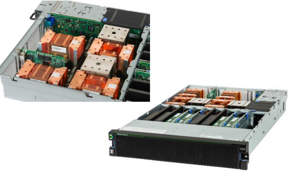
The new HPC platform developed by IBM, NVIDIA and Wistron (which is one of the major contract makers of servers) is based on several IBM POWER8 processors and several NVIDIA Tesla P100 accelerators. At present, the three companies do not reveal a lot of details about their new HPC platform, but it is safe to assume that it has two IBM POWER8 CPUs and four NVIDIA Tesla P100 accelerators. Assuming that every GP100 chip has four 20 GB/s NVLink interconnections, four GPUs is the maximum number of GPUs per CPU, which makes sense from bandwidth point of view. It is noteworthy that NVIDIA itself managed to install eight Tesla P100 into a 2P server (see the example of the NVIDIA DGX-1).

Correction 4/7/2016: Based on the images released by the OpenPOWER Foundation, the prototype server actually includes four, not eight NVIDIA Tesla P100 cards, as the original story suggested.
IBM’s POWER8 CPUs have 12 cores, each of which can handle eight hardware threads at the same time thanks to 16 execution pipelines. The 12-core POWER8 CPU can run at fairly high clock-rates of 3 – 3.5 GHz and integrate a total of 6 MB of L2 cache (512 KB per core) as well as 96 MB of L3 cache. Each POWER8 processor supports up to 1 TB of DDR3 or DDR4 memory with up to 230 GB/s sustained bandwidth (by comparison, Intel’s Xeon E5 v4 chips “only” support up to 76.8 GB/s of bandwidth with DDR4-2400). Since the POWER8 was designed both for high-end servers and supercomputers in mind, it also integrates a massive amount of PCIe controllers as well as multiple NVIDIA’s NVLinks to connect to special-purpose accelerators as well as the forthcoming Tesla compute processors.
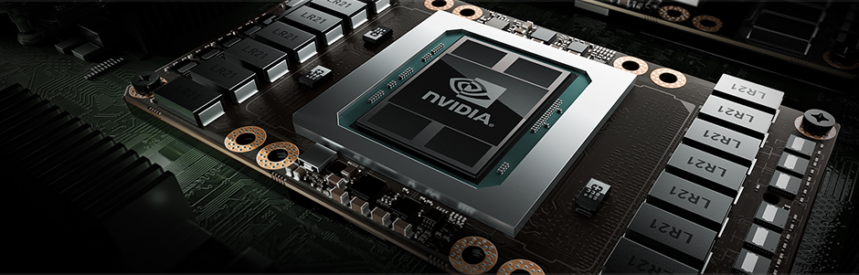
Each NVIDIA Tesla P100 compute accelerator features 3584 stream processors, 4 MB L2 cache and 16 GB of HBM2 memory connected to the GPU using 4096-bit bus. Single-precision performance of the Tesla P100 is around 10.6 TFLOPS, whereas its double precision is approximately 5.3 TFLOPS. A HPC node with eight such accelerators will have a peak 32-bit compute performance of 84.8 TFLOPS, whereas its 64-bit compute capability will be 42.4 TFLOPS. The prototype developed by IBM, NVIDIA and Wistron integrates four Tesla P100 modules, hence, its SP performance is 42.4 TFLOPS, whereas its DP performance is approximately 21.2 TFLOPS. Just for comparison: NEC’s Earth Simulator supercomputer, which was the world’s most powerful system from June 2002 to June 2004, had a performance of 35.86 TFLOPS running the Linpack benchmark. The Earth Simulator consumed 3200 kW of POWER, it consisted of 640 nodes with eight vector processors and 16 GB of memory at each node, for a total of 5120 CPUs and 10 TB of RAM. Thanks to Tesla P100, it is now possible to get performance of the Earth Simulator from just one 2U box (or two 2U boxes if the prototype server by Wistron is used).
IBM, NVIDIA and Wistron expect their early second-generation HPC platforms featuring IBM’s POWER8 processors to become available in Q4 2016. This does not mean that the machines will be deployed widely from the start. At present, the majority of HPC systems are based on Intel’s or AMD’s x86 processors. Developers of high-performance compute apps will have to learn how to better utilize IBM’s POWER8 CPUs, NVIDIA Pascal GPUs, the additional bandwidth provided by the NVLink technology as well as the Page Migration Engine tech (unified memory) developed by IBM and NVIDIA. The two companies intend to create a network of labs to help developers and ISVs port applications on the new HPC platforms. These labs will be very important not only to IBM and NVIDIA, but also to the future of high-performance systems in general. Heterogeneous supercomputers can offer very high performance, but in order to use that, new methods of programming are needed.
The development of the second-gen IBM POWER8-based HPC server is an important step towards building the Summit and the Sierra supercomputers for Oak Ridge National Laboratory and Lawrence Livermore National Laboratory. Both the Summit and the Sierra will be based on the POWER9 processors formally introduced last year as well as NVIDIA’s upcoming code-named Volta processors. The systems will also rely on NVIDIA’s second-generation NVLink interconnect.
Image Sources: NVIDIA, Micron.
Source: OpenPOWER Foundation


50 Comments
View All Comments
Kevin G - Friday, April 8, 2016 - link
@Brutalizer"And here we go again. In think in ALL benchmarks I showed you, EVERY SINGLE ONE OF THEM, you have rejected them all because of this or that.
[...]
The Power8 STREAM numbers are from IBM themselves, as KevinG supplied in the link."
Don't you think it is a bit hypocritical to cite me since two posts below this you call me a troll, that I'm not serious and that "I don't know what I'm talking about"?
Also the link I supplied ( https://blogs.oracle.com/BestPerf/resource/stream/... ) if you haven't noticed is from Oracle, not IBM. If "Oracle" in the URL wasn't a big enough hint, the disclaimer on the first page of that PDF indicates that it was Oracle doing the testing themselves. That PDF is Oracle's detailed testing configuration and as I pointed out, omits a few technical details that are relevant to memory bandwidth. IE we don't know how many DIMMs were installed in the S824. This is a very fair criticism of Oracle's testing and disclosure since it directly impacts performance.
Brutalizer - Friday, April 8, 2016 - link
@Kevin GSorry but I can not "discuss" with you, as you
1) are not serious.
2) trolling.
3) have no clue about the stuff you talk about.
For instance we had a "discussion" about the SGI UV2000 server, that is only used for scale-ou clustered HPC like workloads - and you vehemently explained UV2000 also was used for scale-up workloads like large POWER or SPARC servers. Scale-up workloads such as SAP can not be run on clusters, it can only be run on scale-up servers (look at the SAP top list). UV2000 is in practice a cluster, and there are no SAP entries for that cluster. Still you insisted UV2000 could replace a large Unix server on SAP. When I asked about proof and links, you answered:
1) You can boot SAP on a UV2000
2) It is probably for you that it is possible to run SAP on UV2000
3) something silly I dont remember
You did not present any links to a customer running SAP on UV2000, no SAP benchmarks, no nothing. I even emailed SGI and asked about customers running SAP on UV2000 and there was NO such customer. And even after all this information, you kept insisting on UV2000 could replace large Unix scale-up servers such as POWER and SPARC. No customer runs SAP on UV2000, they only run clustered workloads on x86 UV2000 Linux server.
And I tried to explain to you why it is not possible to run SAP on a cluster: it is because the code branches everywhere, and I gave you links to SGI where they confirm this. And you asked several times "what does it mean when code branches everywhere" and finally I explained in a long essay that ERP software serves 1000s of clients so the server is doing lot of things simultaneously: accounting, book keeping, pay rolls, etc - so the code can never be cached. All these clients are doing all sorts of things, so the code branches everywhere, cache is not that important in scale-up servers. That is why SPARC M7 has a brutal bandwidth, and not so good cache. Bandwidth is more important in scale-up servers than cache.
OTOH, clusters run HPC workloads, that is, run a tight for loop with calculations on the same set of grid points, so the code does not branch, you can cache it well. Cache is important, as the software seldom goes out to RAM. So bandwidth is not important. And if you look at x86 it has low bandwidht and good cache, making it useless for scale-up workloads.
Scale-up workloads thrash the cache. That is why UV2000 can not be used for SAP. I wrote a long essay explaining all this about cache and RAM etc etc. And still after this long explanation, you still did not understand anything about thrashing the cache. You kept writing stuff that showed you did not understand anything why a cluster can not run tightly coupled software.
So, it is useless to try to explain you how things really are. You are given links and explanations, and still you dont get it. You are just very uneducated about computer tech. That makes it difficult to talk to you, because you dont get it, when someone show you links or explain why you are wrong. You dont understand.
Or, you do understand but pretend not to, so you are Trolling to make me write long texts to you. I cant decide which. If you are trolling and pretending to be obtuse, or if you are obtuse for real.
Anyway, I advise anyone to not go into technical discussions with you, because you dont understand what you are talking about. If I point out an error in your post, you dont get it. I even post links, and you read them, and STILL you dont get it. I used to say "there are no dumb people, only ignorant" - but in your case, I am not really sure anymore...
JohnMirolha - Wednesday, April 6, 2016 - link
Actually POWER8 has 320GB/s with a 2 SOCKET system (check link below pg 15)... so it would be 160GB/s per physical chip (you know, despite whatever concept you have, the silicon thing you can pick and plug on a socket).The POWER8 for 2 SOCKET machines is rated at 192GB/s, while his HIGH-END counterpart is rated at 230GB/s. So the difference here is only 16%.
And... who on earth still considers a closed platform like SPARC an HPC alternative ? The only SPARC there is K Computer, which is Fujitsu's SPARC64.
http://openpowerfoundation.org/wp-content/uploads/...
Brutalizer - Thursday, April 7, 2016 - link
So the 2-socket 10-core POWER8 S822L server has 320 GB/s bandwidth? So therefore ONE power8 cpu has 160GB/sec? Well, this again shows how ugly and FUDing the IBM people are.This S822L server has two sockets, but FOUR cpus. So one socket has 160 GB/sec but one POWER8 cpu has 80 GB/sec. You knew this, and tried to trick me into believing that one POWER8 cpu is as fast as SPARC M7. That is the reason you talk about "physical chip..." nonsense.
First I actually wrote a post acknowledging that the POWER8 cpu's bandwidth is as high as SPARC M7, but as I wanted to add a small detail I checked it up, and lo and behold, the S88L server has FOUR cpus. Very very ugly of you. Why am I not surprised by the IBM people? You do know that the term FUD was coined by one of IBM customers?
https://en.wikipedia.org/wiki/Fear,_uncertainty_an...
And finally, if you read the link (it is a research paper) you gave me, it says that the researchers ran the STREAM benchmark 1,000 times, and 10% of the time, the POWER8 server reached 320GB/sec. The rest of the time that is, 23% of the time the benchmark reached 245GB/sec, and 16% of the time it reached 260GB/sec and 24% of the time it reached 290GB/sec. So, only a very small fraction of the time the POWER8 reached 320GB/sec.
So, 10% of the time FOUR power8 cpus reached the same bandwidth as two SPARC M7. The rest of the time, it was far lower. POWWER8 ram bandwidth is not impressive nowhere.
And regarding "And... who on earth still considers a closed platform like SPARC an HPC alternative ?"
Well, have you heard about OpenSPARC which is GNU licensed? Is POWER8 open as in GNU? No? Aha.
https://en.wikipedia.org/wiki/OpenSPARC
.
And if you really want HPC, then SPARC M7 is the fastest computing cpu out there, reaching 1200 SPECint2006 and 832 SPECfp2006. Whereas POWER8 reaches 642 SPECint2006 and 468 SPECfp2006 which is slower than x86 actually. I dont understand why POWER8 is much more expensive than a x86 whilst being slower? Here are 25ish benchmarks where SPARC M7 is 2-3x faster than POWER8 and Intel Xeon E5-2699v3 (all the way up to 11x faster):
https://blogs.oracle.com/BestPerf/entry/201510_spe...
jesperfrimann - Friday, April 8, 2016 - link
RTFM Kebabbert.Read section 2.2 in http://www.redbooks.ibm.com/redpapers/pdfs/redp513...
Each socket in a S824(L or no L) has 8 memory channels, putting a DCM module (dual chip module) as in the or a single chip module or a Quad chip module (if such a thing existed for POWER8), will all give you the same memory bandwidth.
You just have to read the documentation... it's all there .. no conspiracy.. no .. magical cheating.
It is amazing that you have keept up your Rant for so many years.
// Jesper
Brutalizer - Friday, April 8, 2016 - link
Fine, but it is still TRUE that in the server that IBM benchmarked, there where FOUR power8 cpus. Not two. So, it does not matter how much you try to dribble away the fact it was FOUR power8 cpus by talking about irrelevant things.It is amazing you still keep on doing dribbling away facts after this many years. I remember when I showed you SPARC T2+ 1.6GHz besting POWER6 4.7GHz benchmarks to which you replied:
-No, the throughput benchmark you show is irrelevant because POWER6 had lower latency. And that is what counts. So, POWER6 is in general faster than SPARC T2+.
Some time later I showed you a benchmark where SPARC T2+ had lower latency, and you replied:
-No, latency is not important. The only thing that is important is throughput, so POWER6 is faster again.
It IS really amazing that you STILL keep on doing this. One would hope you have matured after all these years. I keep on showing you benchmark after benchmark, which you all reject because of this or that. And when you show me benchmarks, I accept them. But still you reject ALL oracle benchmarks "cherrypicking, etc etc" and when you show me IBM benchmarks you expect me to accept them all. Which I do. And I have asked you why I must accept your benchmarks, but why you reject my benchmarks - to which you reply "Oracle cherrypicking".
Enough of this, I am very well aware of your "debate" technique since many years back. Show us benchmarks where IBM POWER8 cpus have higher RAM bandwidth than SPARC M7. Show us facts and hard numbers, that is what counts. Not your dribbling of facts. If you can not show benchmarks, then I suggest you ventilate your opinions on IBM fan pages instead.
.
And besides, the benchmark I posted, where Oracle compares SPARC M7 to POWER8 in STREAM bandwidth, to which some imply that Oracle lie about the POWER8 result - well that POWER8 result is from IBM themselves. Read the Oracle link and see the reference points to IBM web page. So, Oracle is not lying about POWER8 results.
jesperfrimann - Friday, April 8, 2016 - link
No. There were 4 processors each with 6 cores and 4 memory channels in the benchmark that Oracle ran.Eh... show you numbers that POWER8 has higher Stream benchmark numbers than a SPARC M7 ?
Kind of hard as there are no official STREAM submissions for neither the M7 nor POWER8.
Now surely the per chip throughput of the M7 is very hard to match, it is IMHO the undisputed king of the hill when it comes to chip throughput. It has around 33% faster throughput on many workloads than the best that POWER8 or Xeons can produce. But Again it comes at a Price that you have to have a large number of threads to exploid the potential of the Moster M7 chip.
And not all applications are able to handle such a huge number of threads (256 for the M7 and up to 96 for POWER8)
We do know, cause IBM releases the numbers, what effect it has running only 1 thread per core on the POWER8 chip. Basically it half the throughput going from 8 threads per core to 1 thread per core. For the M7 with it's simpler HW threading the impact surely must be much bigger.
Again reality is more complex than your carmagazine IT World.
// Jesper
jasonelmore - Wednesday, April 6, 2016 - link
anyone remember how Maxwell was supposed to include x64 ARM cores on the flagship GPU's to accelerate performance? It quietly fell off the roadmap about 6 months before maxwell 1 released.HighTech4US - Thursday, April 7, 2016 - link
Only an idiot like you believe every idiotic rumor on the web and believe that it must be true.Kevin G - Thursday, April 7, 2016 - link
It wasn't a rumor:http://www.computerworld.com/article/2493074/compu...
They did have this on their roadmap several years ago. Between Project Denver being lack luster and TSMC's 20 nm process not being suitable for large GPUs, nVidia's roadmaps has radically changed since then. In fact, Pascal wasn't even part of nVidia's roadmap then:
http://www.anandtech.com/show/6846/nvidia-updates-...